

Light emitting device and manufacturing method thereof
a technology of light emitting devices and manufacturing methods, which is applied in the manufacturing of semiconductor/solid-state devices, semiconductor devices, electrical devices, etc., can solve the problems of uneven brightness of one light emitting device, difficulty in making the emission brightness of led elements uniform all the time, etc., and achieve the effect of reducing brightness or emission color variations and brightness unevenness
- Summary
- Abstract
- Description
- Claims
- Application Information
AI Technical Summary
Benefits of technology
Problems solved by technology
Method used
Image

Examples
embodiment 1
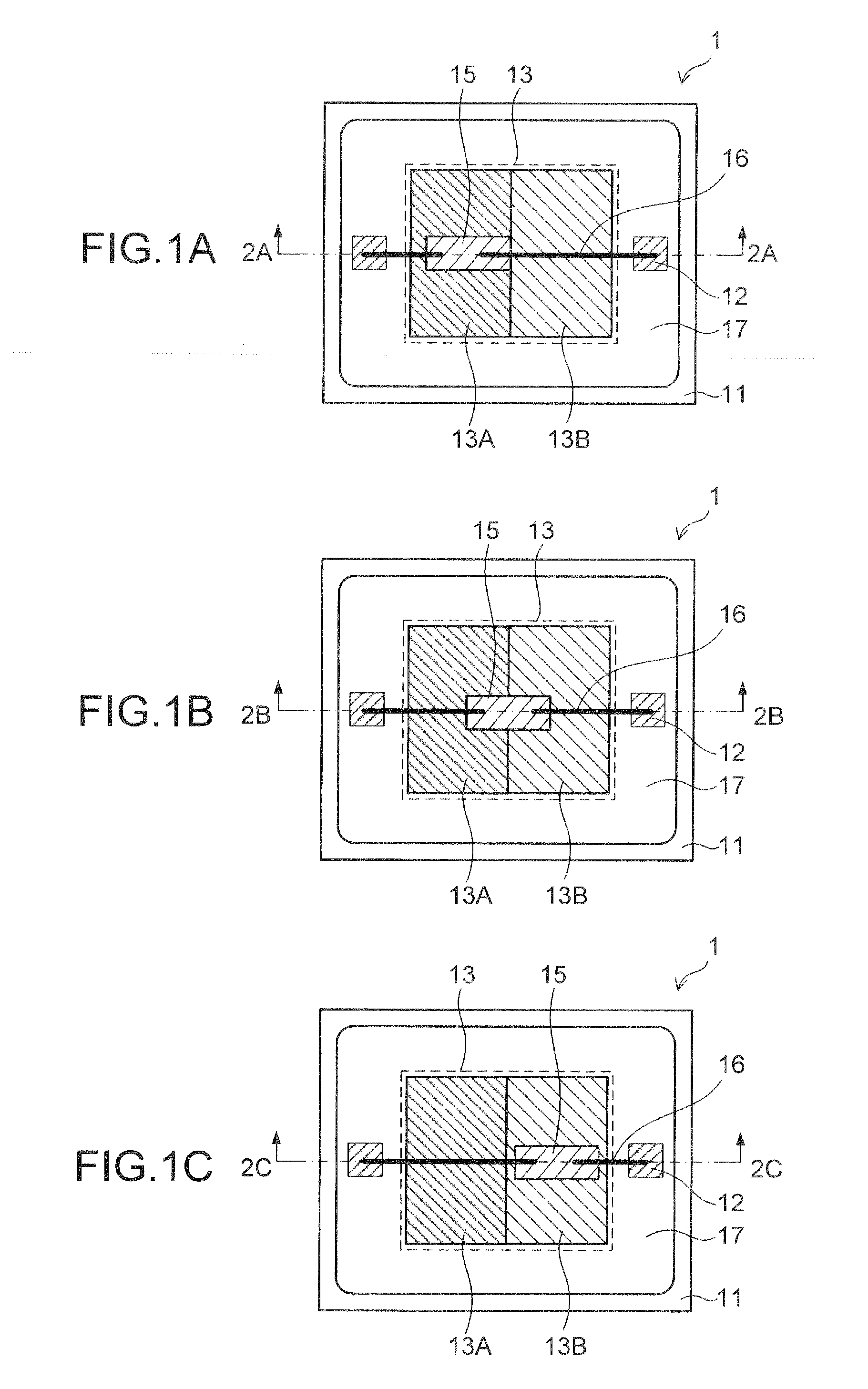
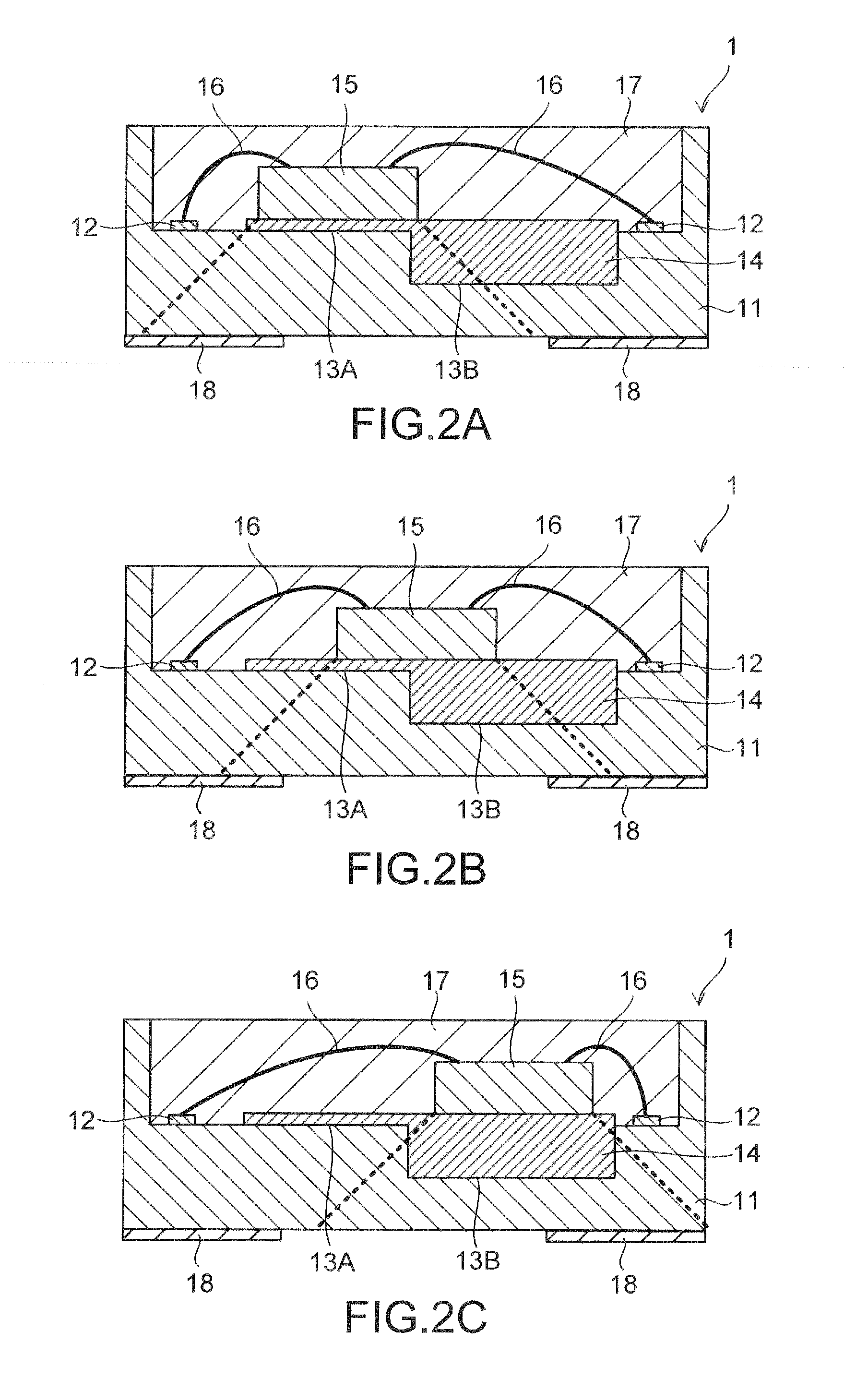
[0037]A light emitting device 1 according to Embodiment 1 of the present invention will be described below with reference to FIGS. 1A-1C and FIGS. 2A-2C. FIGS. 1A to 1C are plan views of the light emitting device 1 as viewed from the light emission surface side.
[0038]The light emitting device 1 is of a single-chip configuration with one LED element 15 mounted on a substrate 11. The substrate 11 is a ceramic substrate made of, for example, Al2O3 (thermal conductivity: 20 W / m·k), and has bonding pads 12 and an element mounting area 13 on its element mounting surface. The LED element 15 is also mounted on the element mounting surface of the substrate 11. The element provision area 13 is defined in the middle of the element mounting surface. The element mounting area 13 has a flat portion 13A defining a flat surface in the principal surface (upper surface) of the substrate 11 and a recess 13B formed in the principal surface of the substrate 11 having a certain depth toward the rear surf...
embodiment 2
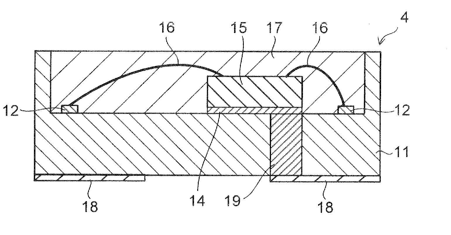
[0057]A light emitting device 2 according to Embodiment 2 of the present invention will be described below with reference to FIG. 4A to FIG. 4C. FIGS. 4A to 4C are cross-sectional views showing the configuration of the light emitting device 2. The light emitting device 2 of Embodiment 2 is similar to the light emitting device 1 of Embodiment 1 in that the element mounting area 13 has a flat portion and a recess, but differs from Embodiment 1 in the configuration of the recess. The light emitting device 2 has a unique recess 13C in Embodiment 2. Similar reference numerals and symbols are used to designate similar parts and elements in Embodiments 1 and 2.
[0058]The recess 13C is adjacent to the flat portion 13A and has a side surface (lateral wall) sloping from the principal surface of the substrate 11 toward the bottom of the recess 13C. That is, the cross-sectional shape of the recess 13C is trapezoidal as shown in FIGS. 4A to 4C. This sloping surface has an inclination angle α (alp...
embodiment 3
[0060]A light emitting device 3 according to Embodiment 3 of the present invention will be described below with reference to FIGS. 5A to 5C and FIGS. 6A to 6C. FIGS. 5A to 5C are plan views of the light emitting device 3 according to Embodiment 3 as viewed from the light emission surface side, and FIGS. 6A to 6C are cross-sectional views taken along the lines 6A-6A, 6B-6B and 6C-6C in FIGS. 5A, 5B and 5C, respectively. Similar reference numerals and symbols are used in Embodiments 1 and 3.
[0061]The light emitting device 3 according to Embodiment 3 differs from the light emitting device 1 according to Embodiment 1 in the configuration of the substrate 11. The configurations of the other parts are the same as those of the light emitting device 1 of Embodiment 1.
[0062]The substrate 11 is made of ceramic such as Al2O3, and has an element mounting area 13 in an element mounting surface of the substrate 11. Bonding pads 12 are provided on the element mounting surface. The element mounting...
PUM
 Abstract
Description
Claims
Application Information