Light emitting device provided with electrically conductive members having high thermal conductivity for thermal radiation

a technology of thermal radiation and electrical conductivity, which is applied in the direction of semiconductor devices for light sources, discharge tubes luminescnet screens, lighting and heating apparatus, etc., can solve the problems of increasing the temperature of the led, reducing the quality of the led device, and reducing the heat conductivity of the substrate. achieve the effect of effective means of heat releas

Inactive Publication Date: 2007-05-15
CITIZEN ELECTRONICS CO LTD
View PDF7 Cites 85 Cited by
  • Summary
  • Abstract
  • Description
  • Claims
  • Application Information

AI Technical Summary

Benefits of technology

[0072]In accordance with the present invention, since the LED is directly mounted on a conductive member having a high heat conductivity, the LED is efficiently cooled. Therefore, the characteristic of the LED is kept so that the reliability of the LED is heightened.

Problems solved by technology

However, the substrate 2 made of resin such as epoxy resin has a very low heat conductivity which is about one-hundredth of that of copper.
Thus, the quality of the LED device largely reduces.
Therefore, the heat is not sufficiently transmitted to the print substrate, thereby rising the temperature of the LED, and reducing the quality thereof.
However, the print substrate is not provided for mounting only the light emitting device, but for mounting other electrical parts such as CPU, memories and others.
To the contrary, such as a print substrate made of metal causes the manufacturing cost of the electric device to increase.

Method used


Image

  • Light emitting device provided with electrically conductive members having high thermal conductivity for thermal radiation
  • Light emitting device provided with electrically conductive members having high thermal conductivity for thermal radiation
  • Light emitting device provided with electrically conductive members having high thermal conductivity for thermal radiation

Examples


first embodiment

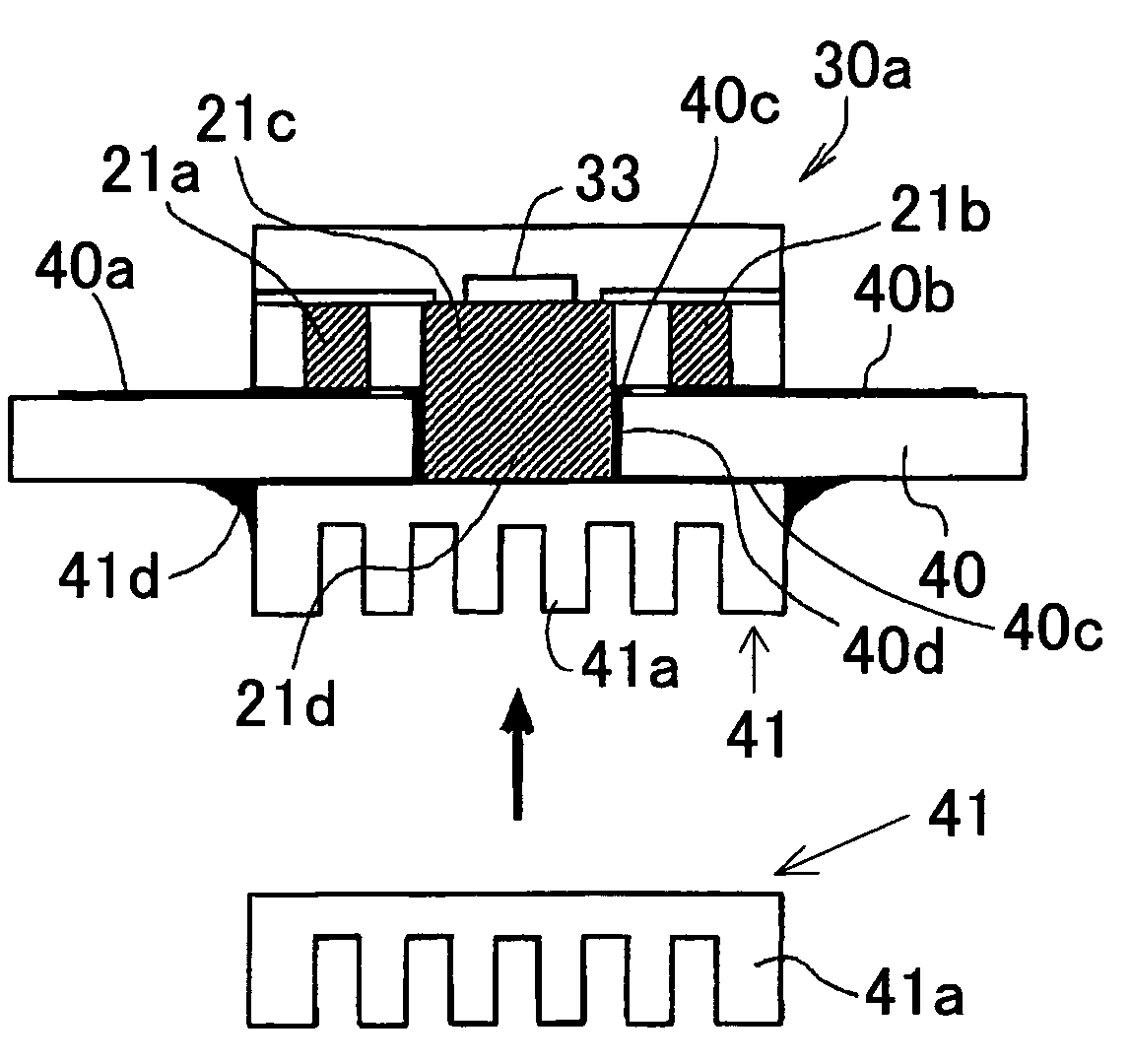
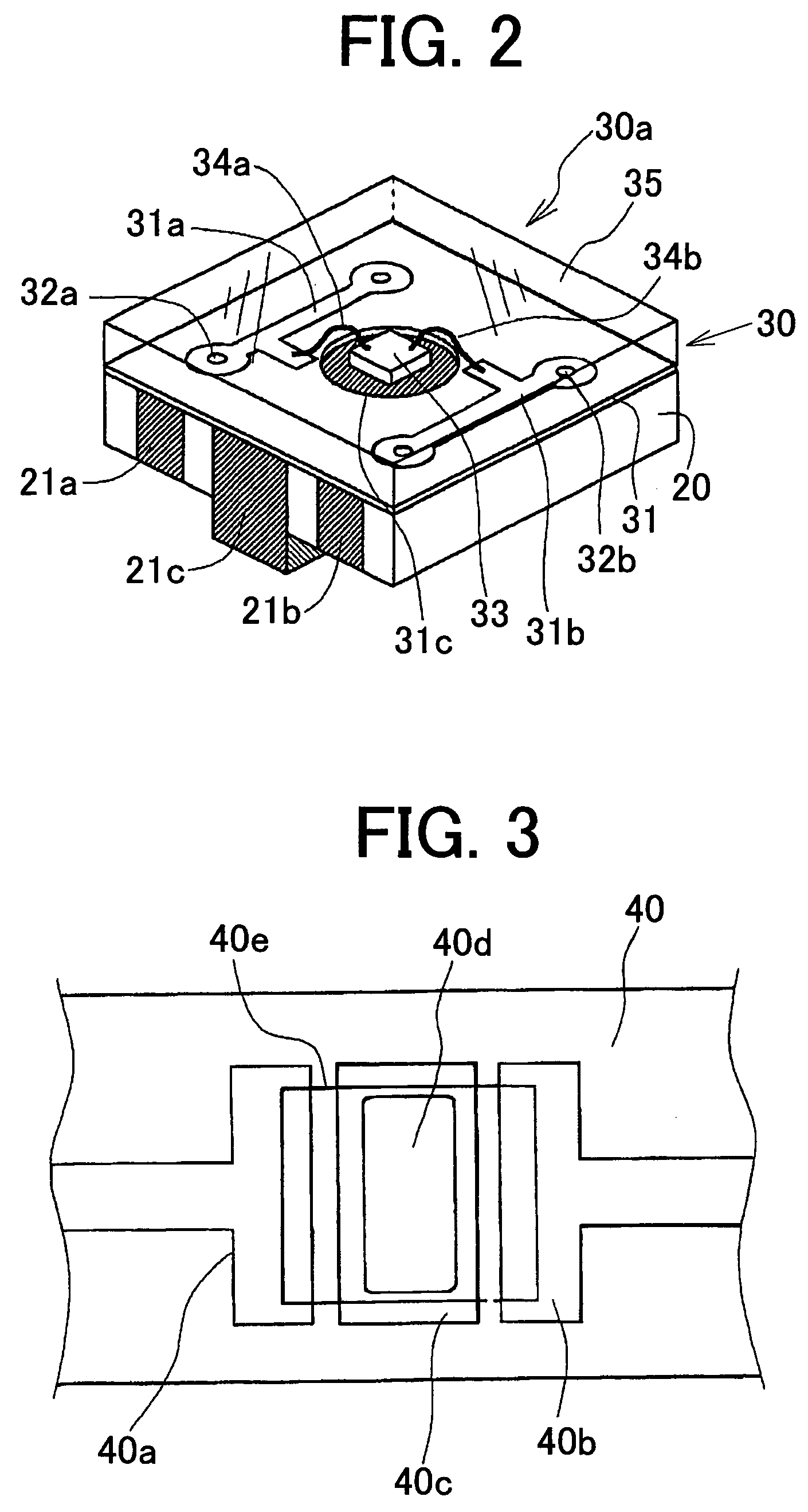
[0044]FIG. 3 is a plan view showing a print substrate used for a light emitting device of the present invention and FIG. 4 is a sectional view of the light emitting device mounted on the print substrate.

[0045]The print substrate 40 has a pair of LED driving patterns 40a and 40b each having a T-shape, and a heat radiation opening 40d having a shape for receiving the lower projection 21d of the heat conductive member 21c. A heat radiation pattern 40c is formed on the surface of the print substrate 40 around the heat radiation opening 40d, on the inside wall of the opening 40d, and on the underside of the print substrate 40.

[0046]As shown in FIG. 4, the opening 40d has a depth equal to the height of the projection 21d. The light emitting device 30a is mounted on the print substrate 40, inserting the projection 21d in the opening 40d.

[0047]The conductive members 21a and 21b are secured to the LED driving patterns 40a and 40b with a solder (not shown). In FIG. 3, a square line 40e show...

third embodiment

[0060]FIG. 9 is a perspective view showing a light emitting device according to the present invention.

[0061]The light emitting device 51 comprises a base member 20a and a light emitting element assembly 30b. The base member 20a comprises the conductive member 21a, a conductive member 21f having heat and electricity conductivity, and insulation members 23e, 23f and 23g. An LED 52 is mounted on the conductive member 21f, so that an electrode on the underside of the LED is connected to the conductive member 21f. The circuit substrate 31 has only the pattern 31a which is connected to an electrode on the LED 52 by the wire 34a. Thus, the LED 52 is electrically connected to the conductive member 21a and electrically and thermally connected to the conductive member 21f as a heat sink.

[0062]In accordance with the third embodiment, since only the single pattern 31a and a pair of conductive members 21a and 21f are provided, the construction is simplified.

[0063]Next, method for manufacturing a...


PUM


Abstract

A light emitting device has a plurality of conductive members with good heat conductivity provided in a base member, the conductive members are isolated by insulating members provided between the conductive members. A light emitting element device is mounted on the base member. An light emitting diode is provided in the light emitting device and mounted on conductive member. A projection is outwardly projected from the heat conductive member for cooling the LED.

Description

BACKGROUND OF THE INVENTION[0001]The present invention relates to a light emitting device using a light emitting diode (LED).[0002]FIG. 16 is a perspective view showing a conventional light emitting device disclosed in Japanese Patent 3,302,203. The light emitting device 1 comprises a substrate 2 made of resin such as epoxy resin, a pair of electrodes 2a and 2b fixed to the substrate 2 at upper and lower side thereof, an LED 3 mounted on the electrode 2a and connected to the electrode 2b by a wire 4, and an sealing member 5 made of a transparent resin for sealing the LED 3.[0003]The light emitting device 1 is mounted on a print substrate 6, connecting the electrodes 2a and 2b with a pair of conductive patterns 6a and 6b. [0004]When current is applied to the LED 3 from the patterns 6a and 6b through the electrodes 2a and 2b, the LED 3 emits light 7.[0005]The thickness of the light emitting device 1 can be reduced because the device is mounted on the print substrate 6 through thin ele...

Claims


Application Information

Patent Timeline
Patent Type & Authority Patents(United States)
IPC IPC(8): H01J61/52F21V29/00H01J1/62H01J63/04H01L33/48H01L33/56H01L33/62H01L33/64
CPCF21V29/75H01L33/642F21V29/74F21V29/004H01L33/486H01L33/641H01L33/647H01L2224/48091H01L2224/48227F21Y2101/02H01L2224/48472H01L2924/00014H01L2924/00F21Y2115/10F21V29/70
Inventor ISODA, HIROTO
Owner CITIZEN ELECTRONICS CO LTD
Why Eureka
Try Eureka