Stack package with improved heat radiation and module having the stack package mounted thereon

a stack package and heat radiation capability technology, which is applied in the direction of electrical equipment, semiconductor devices, semiconductor/solid-state device details, etc., can solve the problems of affecting the production rate of whole stack of semiconductor chips, affecting the production rate of faulty chips, and being unable to repair, so as to achieve the effect of improving heat radiation capability

Inactive Publication Date: 2005-06-23
SAMSUNG ELECTRONICS CO LTD
View PDF10 Cites 86 Cited by
  • Summary
  • Abstract
  • Description
  • Claims
  • Application Information

AI Technical Summary

Benefits of technology

[0016] An exemplary embodiment of the present invention is directed to a stack package with improved heat radiation capability.

Problems solved by technology

Unfortunately, 3-D type semiconductor packaging technologies based on chip stacking have negatively impacted production rates.
For example, faulty chips can dramatically impact production rates because a single faulty chip among a stack of semiconductor chips will cause the whole stack of semiconductor chips to be faulty and non-repairable.
Chips are typically unable to be validated until they are included in a package.
Unfortunately, the heat radiation capability of the heat sink 57 may be hindered by a reduced space (t3), and thus reduced air flow between the modules 50.
Moreover, the heat sink 57 is typically attached to the top surface of the package body 26 that has low heat conductivity, thus further limiting the effect of the heat sink 57.
Another problem related to the heat caused by the semiconductor chips and the difficulty in radiating the heat away from the semiconductor chips, is that the bond between the stack package 10 and the module substrate 51 may be weakened by thermal stress.

Method used


Image

  • Stack package with improved heat radiation and module having the stack package mounted thereon
  • Stack package with improved heat radiation and module having the stack package mounted thereon
  • Stack package with improved heat radiation and module having the stack package mounted thereon

Examples


first embodiment

[0047]FIG. 7 is a plane view of a module 100 in accordance with the present invention, in which the stack packages 60 of FIG. 4 are mounted on a module substrate 101. FIG. 8 is a cross-sectional view taken along the line of VIII-VIII of FIG. 7.

[0048] Referring to FIGS. 7 and 8, the module 100 comprises the module substrate 101. FIG. 8 is a cross-sectional view taken along the line of VIII-VIII of FIG. 7.

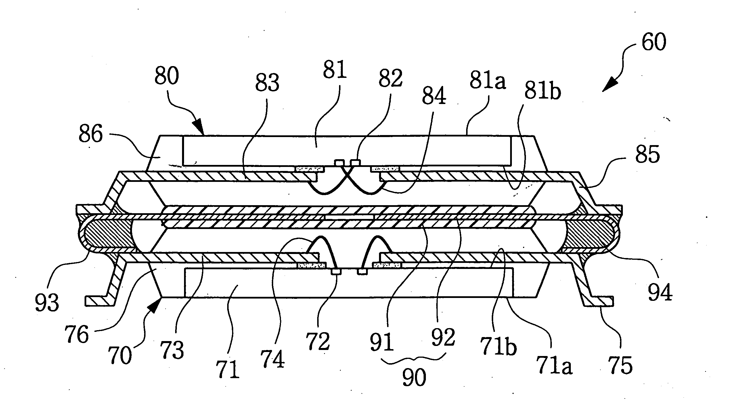
[0049] Referring to FIGS. 7 and 8, the module 100 comprises the module substrate 101, on one surface of which a plurality of stack packages 60 are mounted at a predetermined interval. The back surface 71a of the first chip 71 is exposed through the bottom surface of the stack package 60. The back surface 81a of the second chip 81 is exposed through the top surface of the stack package 60. Therefore, heat which the first and second chips 71 and 81 may generate during operation of the module 100 will be radiated effectively through the top and bottom surfaces of the stack package 60. ...

second embodiment

[0051]FIG. 9 is a cross-sectional view of a module 200 in accordance with the present invention, in which a heat sink 207 is attached to the stack package 60 of FIG. 4 mounted on a module substrate 201. Referring to FIG. 9, the module 200 comprises the heat sink 207 attached to the top surface of the stack package 60. As described above, the stack package 60 is thinner than the conventional stack package. The space between modules 200 is greater with the attached heat sink than the space between modules of the conventional stack package with an attached heat sink. Therefore, the problem of poor flow of air due to reduced space between the modules 200 is mitigated. Thus, the heat sink 207 may provide a good heat radiating characteristic without being hindered by a lack of air flow.

[0052] The heat sink 207 may be made of materials having a high heat conductivity, for example iron, aluminum, copper, ferrous alloy or copper alloy. The heat sink 207 may include a heat conductive member c...

third embodiment

[0053]FIG. 10 is a cross-sectional view of a module 300 in accordance with the present invention. FIG. 11 is an enlarged view of section A of FIG. 10. FIG. 12 is a bottom view of a first chip 71 of FIG. 10.

[0054] Referring to FIGS. 10 through 12, the module 300 comprises a module substrate 301 and a solder bonding portion 303. The stack package 60 is mounted on the module substrate 301. The solder bonding portion 303 is disposed between the bottom surface of the stack package 60 and the top surface of the module substrate 301. The solder bonding portion 303 is formed during a solder reflow process mounting the stack package 60 on the module substrate 301.

[0055] The formation of the solder bonding portion 303 may allow an improved heat radiation capability through the bottom surface of the stack package 60 as well providing a good solder bond between the stack package 60 and the module substrate 301.

[0056] The solder bonding portion 303 includes solder bonding layers 64 and 304 and...


PUM


Abstract

A stack package with improved heat radiation capability and a module having the stack package mounted thereon are provided in which the back surfaces of first and second chips are exposed through the bottom and top surfaces of the stack package, allowing improved heat radiation capability as well as reduced thickness of the stack package. A heat sink may be attached to the stack package for increasing heat radiation capability. A solder bonding portion may be formed between the stack package and a module substrate, establishing good solder bondability between the stack package and the module substrate.

Description

RELATED APPLICATION [0001] This U.S. non-provisional application claims priority under 35 U.S.C. §119 from Korean Patent Application No. 2003-92706 filed on Dec. 17, 2003, the entire contents of which are hereby incorporated by reference. BACKGROUND OF THE INVENTION [0002] 1. Field of the Invention [0003] The present invention relates to a stack package with improved heat radiation capability and a module having the stack package mounted thereon. [0004] 2. Description of the Related Art [0005] Semiconductor products that are lighter, smaller and thinner, and include a great capacity of total memory continue to be desirable. In order to increase the memory capacity of semiconductor products while decreasing their size, technology that can arrange semiconductor memory chips more densely per area of semiconductor substrate used is necessary. One solution has been 3-D type semiconductor packaging technologies based on stacking semiconductor chips. [0006] Examples of 3-D stack chip packa...

Claims


Application Information

Patent Timeline
Patent Type & Authority Applications(United States)
IPC IPC(8): H01L25/18H01L23/12H01L23/495H01L25/10H01L25/11
CPCH01L23/4951H01L2224/73215H01L2224/48091H01L2224/48247H01L2224/4826H01L2224/49175H01L2924/01078H01L2924/01079H01L25/105H01L2224/32245H01L2225/1094H01L2225/107H01L24/48H01L24/49H01L2924/18165H01L2225/1029H01L2225/1041H01L2924/00014H01L2924/00H01L2224/45099H01L2224/45015H01L2924/207H01L23/12
Inventor BAEK, JOONG-HYUNSONG, YOUNG-HEEPARK, SANG-WOOK
Owner SAMSUNG ELECTRONICS CO LTD
Why Eureka
Try Eureka