FET Nanopore Sensor

a nanopore sensor and transistor technology, applied in the field of field effect transistor based sensors, can solve the problems of laborious and expensive application of coatings, difficult fabrication of such sensors, and inability to cover the sensing surface of sensors

Active Publication Date: 2011-11-17
GLOBALFOUNDRIES US INC
View PDF3 Cites 85 Cited by
  • Summary
  • Abstract
  • Description
  • Claims
  • Application Information

AI Technical Summary

Benefits of technology

[0004]In one aspect, a method of using a sensor comprising a field effect transistor (FET) embedded in a nanopore includes placing the sensor in an electrolyte comprising at least one of biomolecules and deoxyribonucleic acid (DNA); placing an electrode in the electrolyte; applying a gate voltage in the sub-threshold regime to the electrode; applying a drain voltage to a drain of the FET; applying a source voltage to a source of the FET; detecting a change in a drain current in the sensor in response to the at least one of biomolecules and DNA passing through the nanopore.
[0005]In one aspect, a method of forming a sensor comprising a field effect transistor (FET) sensor embedded in a nanopore includes epitaxially growing a FET stack comprising a source layer, a drain layer, and a channel layer on a silicon on insulator (SOI) wafer; forming a top silicon nitride layer over the FET stack; forming a bottom silicon nitride layer under the SOI wafer; forming a window in the bottom silicon nitride and the SOI wafer; forming a nanopore in the FET stack; and coating the nanopore with a gate dielectric to form the FET sensor.
[0006]In one aspect, a method of forming a sensor comprising a field effect transistor (FET) sensor embedded in a nanopore includes forming a silicon membrane; forming an oxide layer on the silicon membrane; forming a first metal layer on a side of the silicon membrane opposite the oxide layer, and a first capping layer over of the first metal layer; removing the oxide layer; forming a second metal layer on a side of the silicon membrane opposite the first metal layer, and a second capping layer over of the second metal layer; annealing the silicon membrane and first and second metal layers to form first and second metal silicide layers on opposite sides of the silicon membrane; removing the first and second capping layers; forming a nanopore through the silicon membrane and the first and second metal silicide layers; and coating the nanopore with a gate dielectric to form the FET sensor.

Problems solved by technology

Fabricating such a sensor is challenging.
For protein and viruses detection, a disadvantage of many FET-based sensors is that a sensing surface of the sensor must to be covered with a biological coating that specifically binds the biomolecules to be detected.
Applying the appropriate coating may be labor intensive and expensive.
Further, the sensor may only be used to detect the particular biomolecules that bind with the coating, limiting the usefulness of the sensor.
However, for protein and viruses detection, a disadvantage of many FET-based sensors is that a sensing surface of the sensor must to be covered with a biological coating that specifically binds the biomolecules to be detected.
Applying the appropriate coating may be labor intensive and expensive.
Further, the sensor may only be used to detect the particular biomolecules that bind with the coating, limiting the usefulness of the sensor.
Though this method is standard for forming source and drain regions in longer channel (greater than 10 nm) FET devices, ion implantation and anneal may pose a problem for fabrication of relatively short FET channel (less than about 5 nm) required for high sensitivity FET devices, as ion implantation and high temperature activation annealing produce dopant density profiles in the source / drain regions that may extend several nanometers into the channel region of the FET.
Consequently, the sensitivity of a FET sensor formed in this manner may be degraded, making the FET sensor inappropriate for use for sequencing DNA.

Method used


Image

  • FET Nanopore Sensor
  • FET Nanopore Sensor
  • FET Nanopore Sensor

Examples


Embodiment Construction

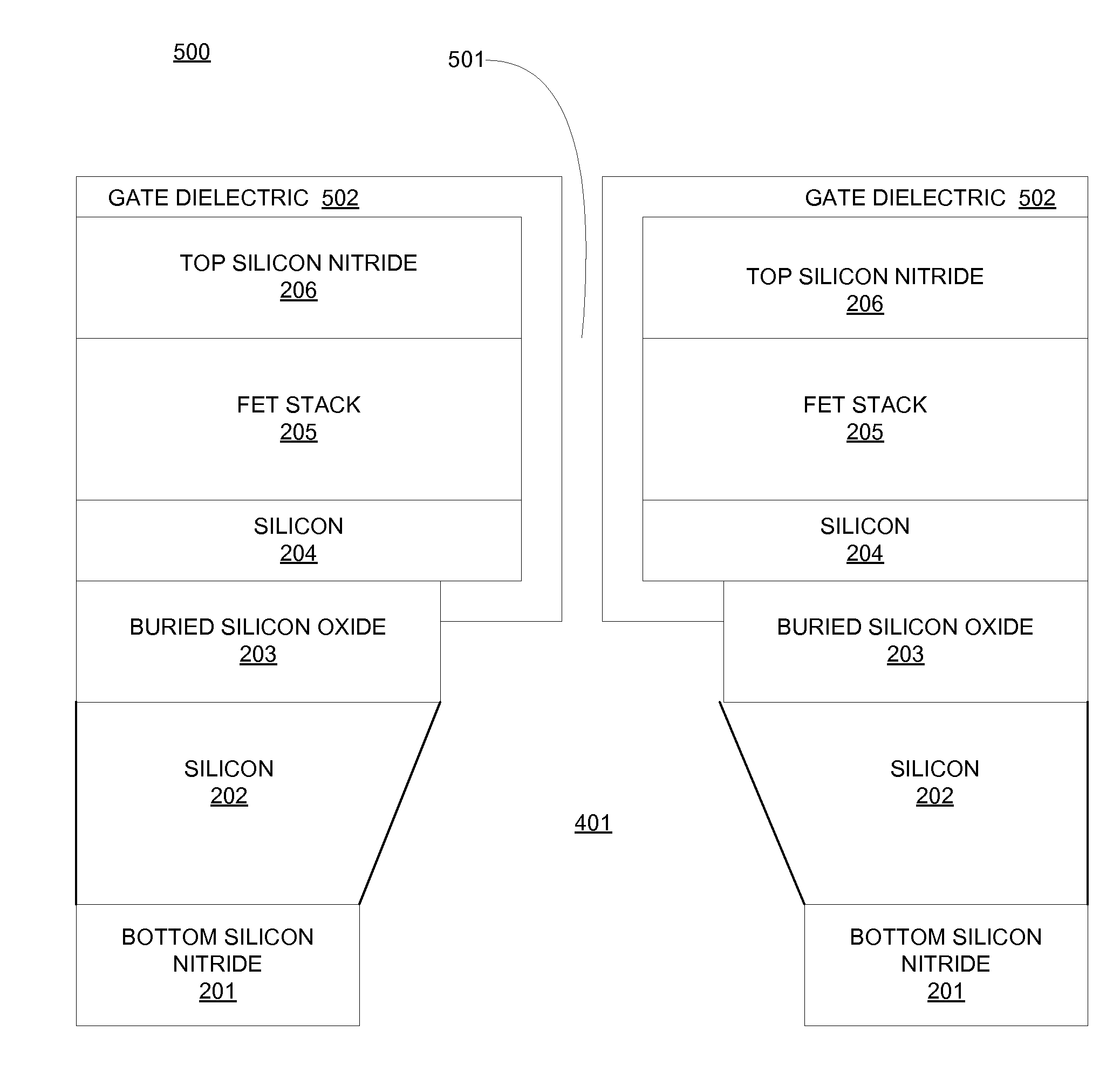
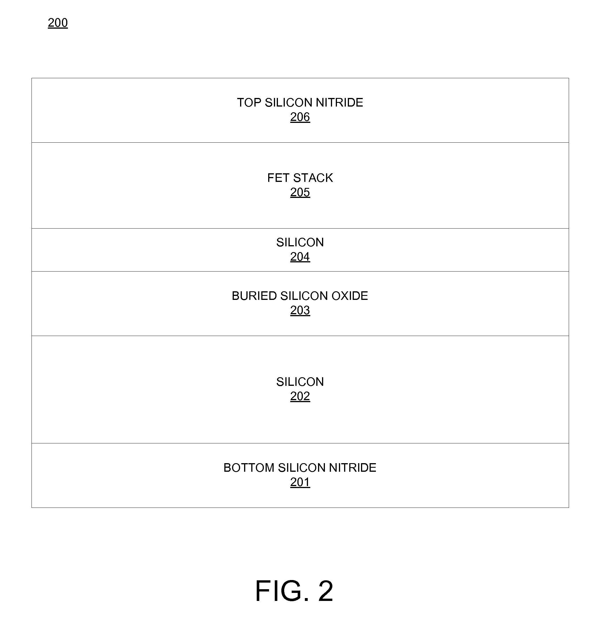
[0024]Embodiments of systems and methods for a FET nanopore sensor are provided, with exemplary embodiments being discussed below in detail. A FET nanopore sensor may be used to detect various types of biomolecules without requiring a sensing surface covered with a biological coating to bind the biomolecules. A FET nanopore sensor may also be used to sequence DNA strands. The FET nanopore sensor may have a relatively short channel length (less than about 3 nm in some embodiments, and less than about 1 nm in some preferred embodiments), so that the sensitivity of the FET nanopore sensor is appropriate for sequencing DNA. The FET nanopore sensor may be fabricated in a manner that results in abrupt junctions between highly doped source and drain regions that are separated by a relatively thin channel region.

[0025]The FET nanopore sensor may comprise a FET stack with a nanopore located in the FET stack. The FET stack comprises a channel region located in between a source and a drain reg...


PUM

PropertyMeasurementUnit
thicknessaaaaaaaaaa
thicknessaaaaaaaaaa
thicknessaaaaaaaaaa

Abstract

A method of using a sensor comprising a field effect transistor (FET) embedded in a nanopore includes placing the sensor in an electrolyte comprising at least one of biomolecules and deoxyribonucleic acid (DNA); placing an electrode in the electrolyte; applying a gate voltage in the sub-threshold regime to the electrode; applying a drain voltage to a drain of the FET; applying a source voltage to a source of the FET; detecting a change in a drain current in the sensor in response to the at least one of biomolecules and DNA passing through the nanopore.

Description

FIELD[0001]This disclosure relates generally to the field of field effect transistor based sensors for sequencing deoxyribonucleic acid (DNA) and proteins. The sensors can also be used for detection of biological molecules such as proteins and viruses.DESCRIPTION OF RELATED ART[0002]Mapping the sequences of bases of a DNA strand is of great importance in life sciences. Since a single base is about 0.7 nanometers (nm) long when the DNA strand is stretched, it is important that a sensor for sequencing has spatial resolution of about 1 nm or less. Fabricating such a sensor is challenging. Another area of great importance in life sciences is detection of proteins and viruses. For protein and viruses detection, a disadvantage of many FET-based sensors is that a sensing surface of the sensor must to be covered with a biological coating that specifically binds the biomolecules to be detected. Applying the appropriate coating may be labor intensive and expensive. Further, the sensor may onl...

Claims


Application Information

Patent Timeline
Patent Type & Authority Applications(United States)
IPC IPC(8): G01N27/06H01L21/02
CPCB82Y15/00G01N27/02G01N27/4145G01N33/48721C12Q1/6825G01N27/3276G01N33/54373
Inventor BEDELL, STEPHEN W.D' EMIC, CHRISTOPHERPENG, HONGBOZAFAR, SUFI
Owner GLOBALFOUNDRIES US INC
Why Eureka
Try Eureka