
Solid-state imaging device

a solid-state imaging and imaging film technology, applied in the direction of semiconductor devices, basic electric elements, electrical equipment, etc., can solve the problems of red light and magenta light leakage light in the optical waveguide leaks into the side of the insulating, so as to enhance the color reproducibility

Inactive Publication Date: 2011-11-24
PANASONIC CORP
View PDF1 Cites 12 Cited by
  • Summary
  • Abstract
  • Description
  • Claims
  • Application Information

AI Technical Summary

Benefits of technology

[0011]Therefore, the present invention has an object to provide a solid-state imaging device which is capable of enhancing color reproducibility.
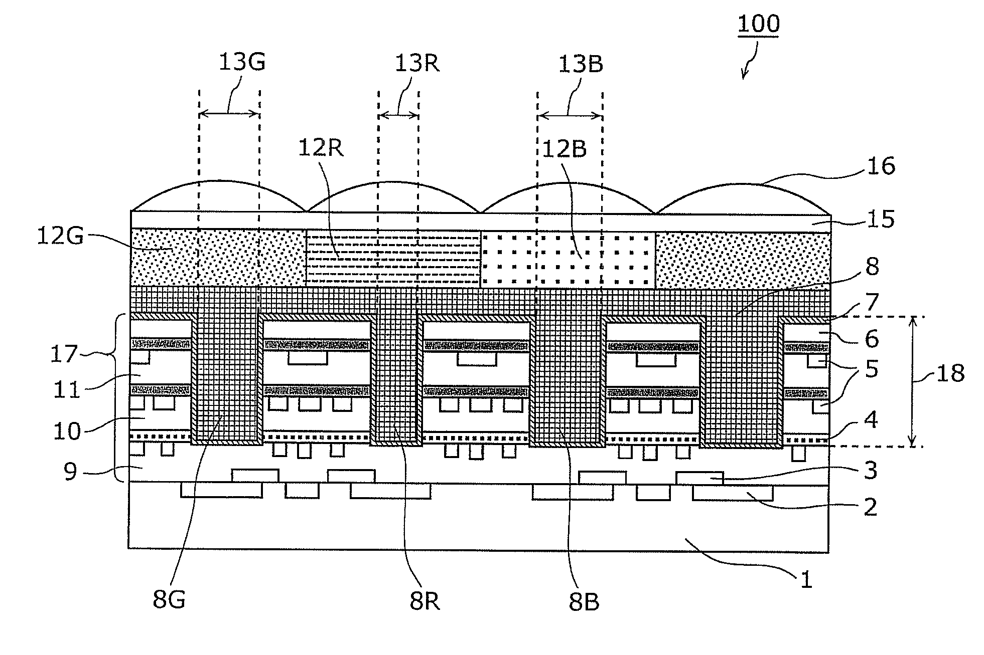
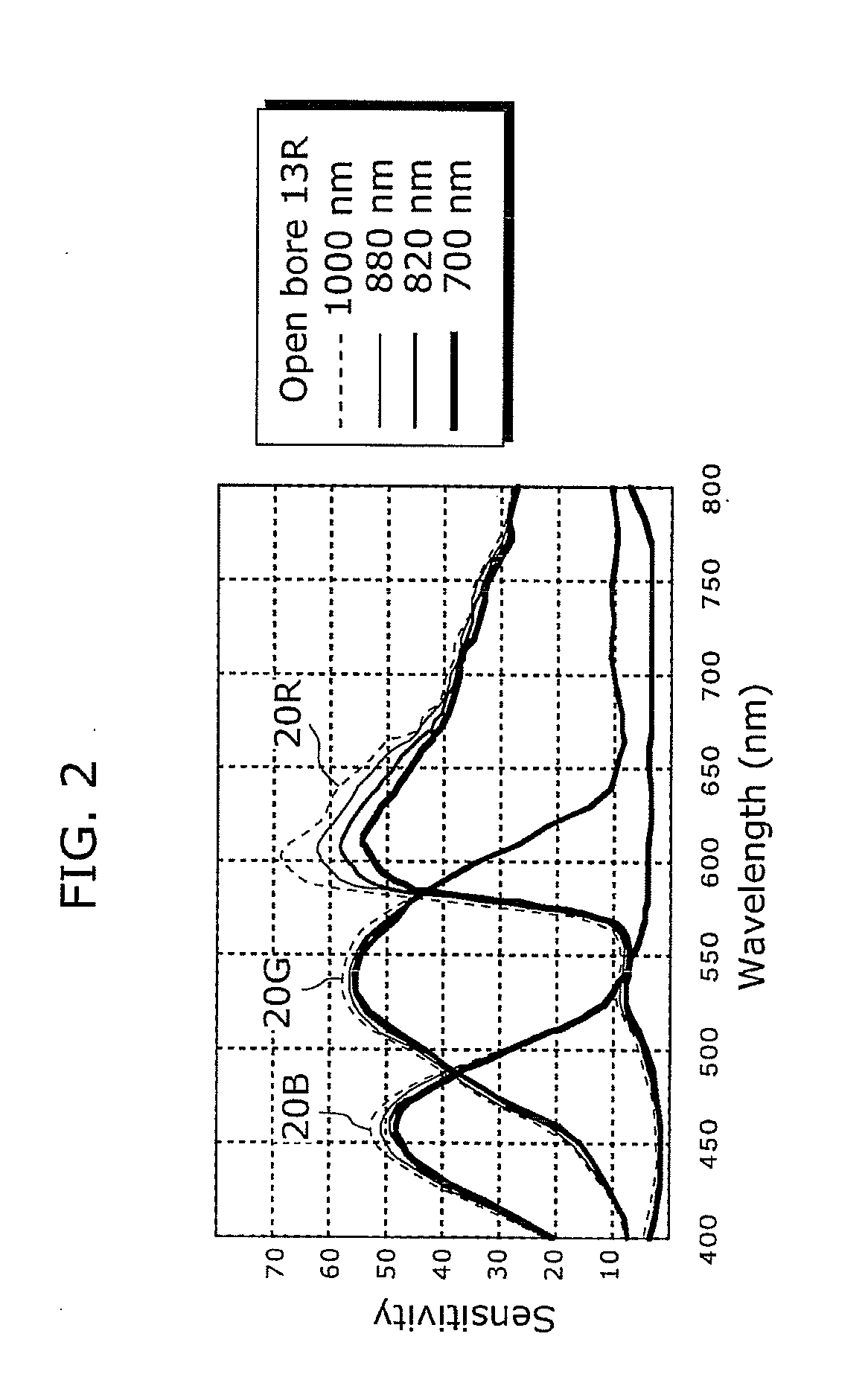
[0013]With this configuration, in the solid-state imaging device according to the aspect of the present invention, the width of the first optical waveguide formed above the first photodiode which receives light having a long wavelength is smaller than the width of the second optical waveguide formed above the second photodiode which receives light having a short wavelength. This successfully increases a distance between the first optical waveguide and other optical waveguides adjacent to the first optical waveguide, and thus it is possible to suppress leakage of the light having the long wavelength in the optical waveguide into adjacent pixels. With this, the solid-state imaging device according to the aspect of the present invention makes it possible to reduce color mixing to the adjacent pixels, thereby enhancing color reproducibility.
[0015]With this configuration, the solid-state imaging device according to the aspect of the present invention makes it possible to suppress leakage of the red light in the optical waveguide into an adjacent pixel which receives the green light or into an adjacent pixel which receives the blue light.
[0017]With this configuration, the solid-state imaging device according to the aspect of the present invention makes it possible to suppress leakage of the magenta or yellow light in the optical waveguide into an adjacent pixel which receives the cyan light or into an adjacent pixel which receives the green light.
[0022]Therefore, the present invention can provide the solid-state imaging device which is capable of enhancing the color reproducibility.FURTHER INFORMATION ABOUT TECHNICAL BACKGROUND TO THIS APPLICATION

Problems solved by technology

However, in the solid-state imaging device in which the optical waveguide which waveguides, to the photodiode, the light incident on the microlens is thus provided, a problem occurs that the light in the optical waveguide leaks into a side of the insulating film.
More specifically, red light leaks into the side of the insulating film when a primary color filter is used, and yellow light and magenta light leak into the side of the insulating film when a complementary color filter is used.
Consequently, a conventional solid-state imaging device has a problem that color mixing to adjacent pixels occurs, which results in deterioration of color reproducibility.

Method used


Image

  • Solid-state imaging device
  • Solid-state imaging device
  • Solid-state imaging device

Examples


embodiment 1

[0037]In a solid-state imaging device 100 according to Embodiment 1 of the present invention, a width of an optical waveguide formed above a photodiode which receives red light is smaller than a width of an optical waveguide formed above a photodiode which receives blue light and a width of an optical waveguide formed above a photodiode which receives green light. This successfully increases a distance between the optical waveguide formed above the photodiode which receives red light and the other optical waveguides adjacent to the optical waveguide, and thus it is possible to suppress leakage of the red light in the optical waveguide into adjacent pixels. With this, the solid-state imaging device 100 according to Embodiment 1 of the present invention makes it possible to reduce color mixing to the adjacent pixels, thereby enhancing color reproducibility.

[0038]The following first describes a structure of the solid-state imaging device 100 according to Embodiment 1 of the present inv...

embodiment 2

[0064]In Embodiment 2, described is a modification of the solid-state imaging device 100 according to Embodiment 1, that is, a solid-state imaging device 100A to which complementary color filters are applied.

[0065]FIG. 11 is a cross-sectional view of the solid-state imaging device 100A according to Embodiment 2 of the present invention. It is to be noted that the same reference signs are assigned to the same elements as in FIG. 1, and an overlapping description is omitted.

[0066]In comparison with the solid-state imaging device 100 shown in FIG. 1, the solid-state imaging device 100A shown in FIG. 11 includes color filters 22C, 22Y, 22G, and 22M instead of the color filters 12R, 12G, and 12B.

[0067]The color filters 22C, 22Y, 22G, and 22M are formed above the interlayer insulating film 17. The color filter 22C transmits cyan light, the color filter 22Y transmits yellow light, the color filter 22G transmits green light, and the color filter 22M transmits magenta light.

[0068]Moreover, a...


PUM


Abstract

A solid-state imaging device according to an aspect of the present invention includes: a first photodiode and a second photodiode; a first optical waveguide formed above the first photodiode; a second optical waveguide formed above the second photodiode; a first color filter which is formed above the first optical waveguide and transmits mainly light having a first wavelength; a second color filter which is formed above the second optical waveguide and transmits mainly light having a second wavelength; a first microlens formed above the first color filter; and a second microlens formed above the second color filter, wherein the first wavelength is longer than the second wavelength, and the first optical waveguide has a first width smaller than a second width of the second optical waveguide, the first and second widths being in a direction parallel to the semiconductor substrate.

Description

BACKGROUND OF THE INVENTION[0001](1) Field of the Invention[0002]The present invention relates to a solid-state imaging device including an optical waveguide.[0003](2) Description of the Related Art[0004]Along with downsizing of cameras and an increase of the number of pixels, miniaturization of cells in solid-state imaging devices has been advanced. As a result, it has become necessary to establish a technique of preventing reduction in photosensitivity that is a key characteristic of the solid-state imaging devices.[0005]Moreover, the advancement of the miniaturization of the cells has made it difficult to manage both the miniaturization of the cells and an increase in sensitivity, using a conventional structure. To advance the miniaturization of the cells and maintain the photosensitivity, it is essential to decrease a distance from a photodiode to the bottom of a microlens. However, especially in a MOS (Metal Oxide Semiconductor) image sensor, a line needs to be formed beside a ...

Claims


Application Information

Patent Timeline
Patent Type & Authority Applications(United States)
IPC IPC(8): H01L31/0232
CPCH01L27/14621H01L27/14645H01L27/14629H01L27/14627
Inventor SAKOH, HIROSHIKATAOKA, MASAOKATSUNO, MOTONARITAKASE, MASAYUKIHIRAI, JUN
Owner PANASONIC CORP
Learn More