3D integrated circuit and method of manufacturing the same

a technology of integrated circuits and manufacturing methods, applied in the direction of electrical equipment, semiconductor devices, semiconductor/solid-state device details, etc., can solve the problems of performance degradation or even fault of integrated circuits, dielectric layers and through-si-vias in integrated circuits will probably be damaged

Active Publication Date: 2011-11-24
INST OF MICROELECTRONICS CHINESE ACAD OF SCI
View PDF12 Cites 201 Cited by
  • Summary
  • Abstract
  • Description
  • Claims
  • Application Information

AI Technical Summary

Benefits of technology

[0014]For semiconductor devices made on silicon on insulator (SOI), bulk Si, or other semiconductor substrate, the diffusion trapping layer for preventing diffusion of the metal ions manufactured by the self-align technology provided by the embodiments of the present invention avoids damages induced to the dielectric layer and the through-Si-via by ion implantation.

Problems solved by technology

In the process of manufacturing an integrated circuit, it is very likely for metal ions such as Cu, Fe, or Na ions from structures such as through-Si-via (TSV), interconnection structure, or metal electrode of semiconductor device, to diffuse into transistor structures and interconnection structures, causing performance degradation or even fault of the integrated circuit.
Particularly, the dielectric layers and the through-Si-vias in the integrated circuit will probably be damaged.

Method used


Image

  • 3D integrated circuit and method of manufacturing the same
  • 3D integrated circuit and method of manufacturing the same
  • 3D integrated circuit and method of manufacturing the same

Examples


Embodiment Construction

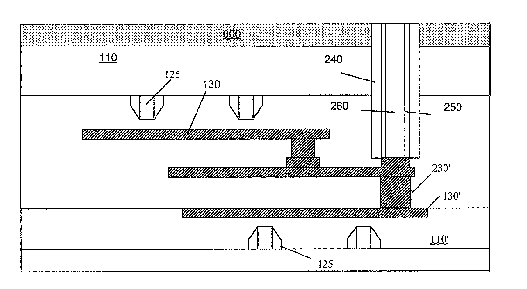
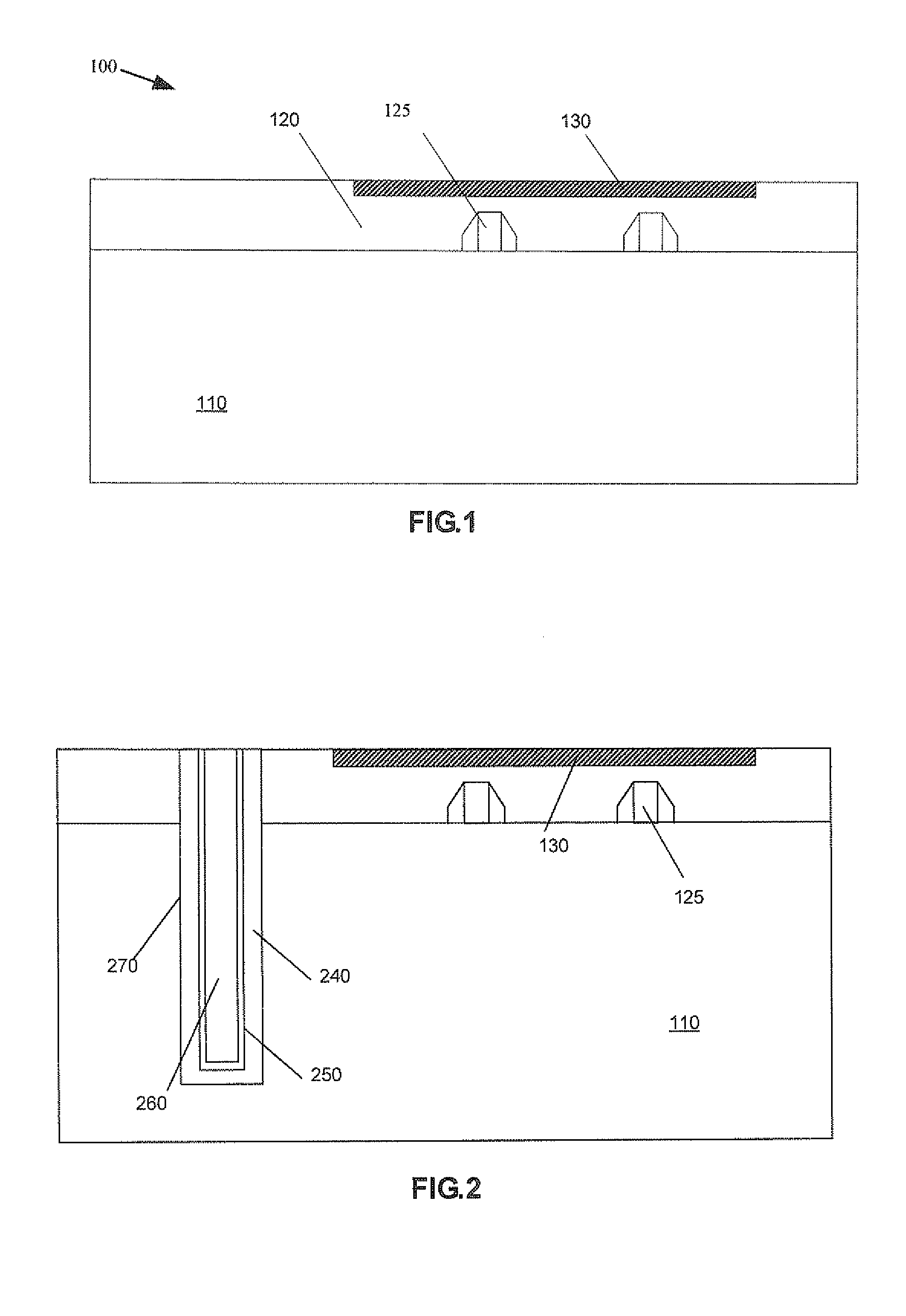
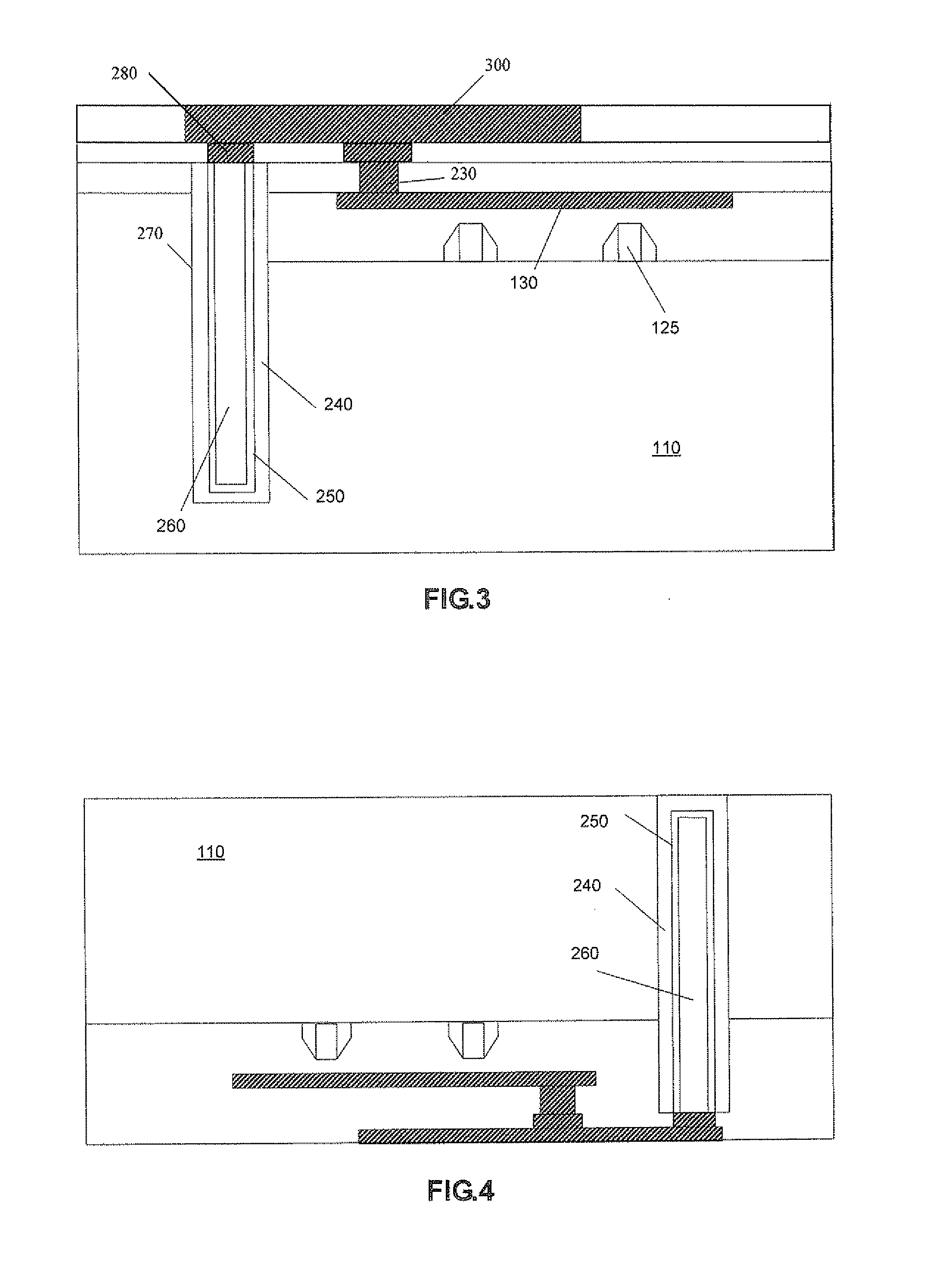
[0016]The following disclosure provides many different embodiments or examples to implement the technical solutions provided by the present invention. The following description describes components and arrangements of specific examples, but they are only exemplary, and are not intended to limit the present invention.

[0017]Further, reference numerals and / or characters may be repeatedly used in various embodiments of the present invention. Such repetitions are for simplicity and clarity purpose, and do not indicate relationships among various embodiments and / or arrangements being discussed.

[0018]The present invention provides examples about various specific process and / or materials, but those skilled in the art may conceive other process and / or other materials for substitution. It is obvious that such substitution will not depart from the scope of the present invention. It should be noted that edges of the regions described herein comprises necessary expansions as required by the proc...


PUM


Abstract

The present invention provides a 3D integrated circuit and a manufacturing method thereof. The circuit structure comprises: a semiconductor substrate; at least one semiconductor device formed on the upper surface of the semiconductor substrate; a through-Si-via through the semiconductor substrate and comprising an insulating layer covering sidewalls of the through-Si-via and conductive material filled in the insulating layer; an interconnection structure connecting the at least one semiconductor device and the through-Si-via; and a diffusion trapping region formed on the lower surface of the semiconductor substrate. The present invention is applicable in manufacture of the 3D integrated circuit.

Description

BACKGROUND OF THE INVENTION[0001]1. Field of the Invention[0002]The invention relates to the field of integrated circuit manufacturing, and more particularly, to an integrated circuit having a diffusion trapping layer and a method of manufacturing the same.[0003]2. Description of the Prior Art[0004]In the process of manufacturing an integrated circuit, it is very likely for metal ions such as Cu, Fe, or Na ions from structures such as through-Si-via (TSV), interconnection structure, or metal electrode of semiconductor device, to diffuse into transistor structures and interconnection structures, causing performance degradation or even fault of the integrated circuit.[0005]The metal ions may be trapped by means of directly implanting ions into the integrated circuit structure. However, the implanted ions may enter regions other than the target regions. Particularly, the dielectric layers and the through-Si-vias in the integrated circuit will probably be damaged.SUMMARY OF THE INVENTIO...

Claims


Application Information

Patent Timeline
Patent Type & Authority Applications(United States)
IPC IPC(8): H01L29/36H01L21/265
CPCH01L21/76898H01L27/0688H01L2924/0002H01L2924/00
Inventor ZHU, HUILONG
Owner INST OF MICROELECTRONICS CHINESE ACAD OF SCI
Why Eureka
Try Eureka