
Image processing method and display device using the same

a display device and image processing technology, applied in the field of image processing method and display device, can solve the problems of complex computational process of this algorithm, increase in product unit cost, and the inability to manufacture the display devi

Active Publication Date: 2011-11-24
LG DISPLAY CO LTD
View PDF8 Cites 8 Cited by
  • Summary
  • Abstract
  • Description
  • Claims
  • Application Information

AI Technical Summary

Benefits of technology

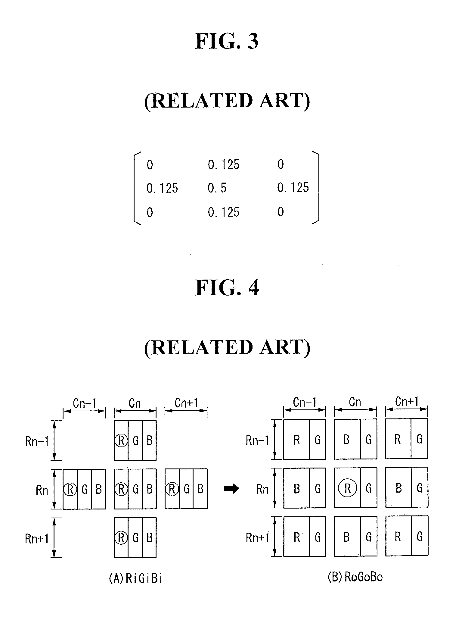
[0009]However, in such conventional technology, an algorithm was developed for a display device, which can be actually be manufactured, has a low resolution. A computational process of this algorithm is complicated because R, G, and B data are all filtered to prevent degradation of a display image. As a result, the degree of reduction of power consumption is small in the actual implementation of a driver IC. Moreover, a color error occurs in a display image due to the diamond filter used for image processing and the sharpness processing using G data, and blurring of the contour of the display image occurs as shown in FIG. 5. Further, as is evident in FIG. 4, particular rows and two rows vertically adjacent thereto are required to determine data values of pixels arranged in the corresponding particular rows, so a minimum of three line memories have to be provided. An increase in line memories causes an increase in product unit cost.

Problems solved by technology

However, in such conventional technology, an algorithm was developed for a display device, which can be actually be manufactured, has a low resolution.
A computational process of this algorithm is complicated because R, G, and B data are all filtered to prevent degradation of a display image.
Moreover, a color error occurs in a display image due to the diamond filter used for image processing and the sharpness processing using G data, and blurring of the contour of the display image occurs as shown in FIG. 5.
An increase in line memories causes an increase in product unit cost.

Method used


Image

  • Image processing method and display device using the same
  • Image processing method and display device using the same
  • Image processing method and display device using the same

Examples


Embodiment Construction

[0027]Hereinafter, an implementation of this document will be described in detail with reference to FIGS. 6 to 13.

[0028]First, an image processing method of the present invention will be described through FIGS. 6 to 11.

[0029]FIG. 6 sequentially shows an image processing method according to an exemplary embodiment of the present invention.

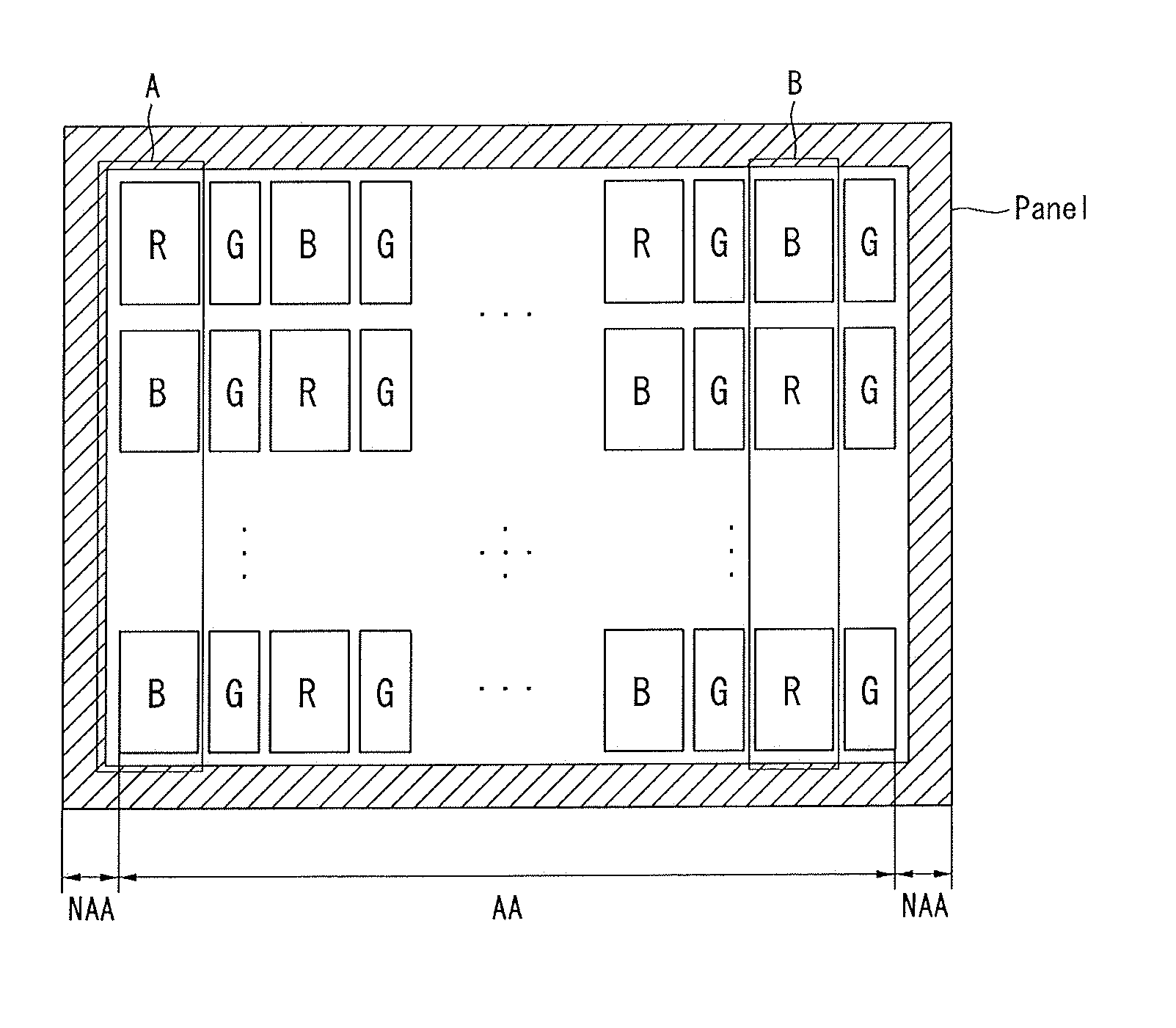
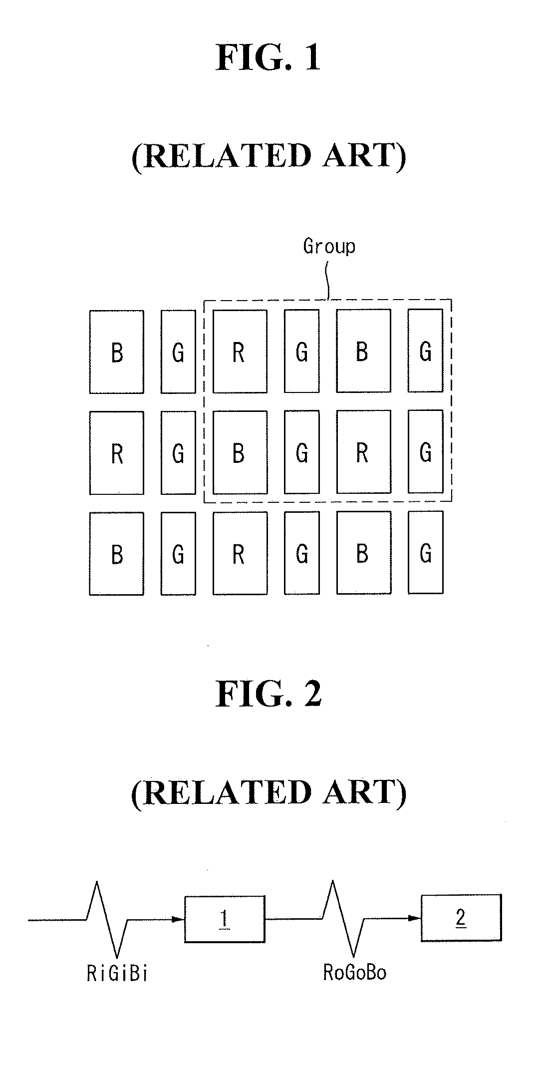
[0030]Referring to FIG. 6, this image processing method is carried out on a display panel whose number of pixels is smaller than the resolution of an input image. In the display panel according to the present invention, there are as many G sub-pixels as the display resolution of input G data and as many R and B sub-pixels as half the display resolution of input R and B data, respectively. In other words, as shown in FIG. 1, the display panel according to the present invention has sub-pixel groups, each sub-pixel group comprising eight sub-pixels: four G sub-pixels; two R sub-pixels; and two B sub-pixels, and repeating in a checkerboard pattern. An R...


PUM


Abstract

An image processing method comprises: (A) separating R and B data and G data from input data; (B) loading data corresponding to respective odd rows of gamma-converted R and B data, and storing data corresponding to respective even rows of the R and B data adjacent to the loaded odd rows; (C) loading two R data of the even row, along with two R data of the odd row corresponding to a first display position, so as to form a 2×2 R pixel area, and loading two B data of the even row, along with two B data of the odd row corresponding to a second display position, so as to form a 2×2 B pixel area; (D) computing the sharpness of the corresponding display data by comparing the data in each of the R and B pixel areas column by column and row by row; (E) computing the luminance of the display data by taking the average value of the data corresponding to the odd row of each of the R and B pixel areas; (F) determining the gray scale value of output R data by adding the sharpness to the luminance of the R data, and determining the gray scale value of output B data by adding the sharpness to the luminance of the B data; and (G) combining the inverse-gamma-converted R and B data and the input G data and then outputting the combined data according to the sub-pixel structure of the display panel.

Description

[0001]This application claims the benefit of the Korean Patent Application No. 10-2010-0047628, filed in Korea on May 20, 2010, which are hereby incorporated by reference as if fully set forth herein.BACKGROUND[0002]1. Field of the Invention[0003]This document relates to an image processing method and a display device using the same.[0004]2. Discussion of the Related Art[0005]Known display devices include a cathode ray tube, a liquid crystal display (LCD), an organic light emitting diode (OLED), a plasma display panel (PDP), etc. Such a display device has as many sub-pixels of red (R), green (G), and blue (B), respectively, as the maximum number of pixels of an image that can be displayed.[0006]In recent years, in order to reduce power consumption and achieve high resolution in a display device, a technology for reproducing an image close to the original image using pixels whose number is smaller than the resolution of an input image was proposed in U.S. Pat. No. 7,492,379, for exam...

Claims


Application Information

Patent Timeline
IPC IPC(8): G09G5/10
CPCG09G3/2003G09G2300/0452G09G2320/0276G09G2340/0457G09G2320/066G09G2340/0421G09G2320/029
Inventor PARK, BYUNGHWEELEE, NAMYANGCREDELLE, THOMAS LIOYD
Owner LG DISPLAY CO LTD
Learn More