Contact force sensor
- Summary
- Abstract
- Description
- Claims
- Application Information
AI Technical Summary
Benefits of technology
Problems solved by technology
Method used
Image

Examples
first embodiment
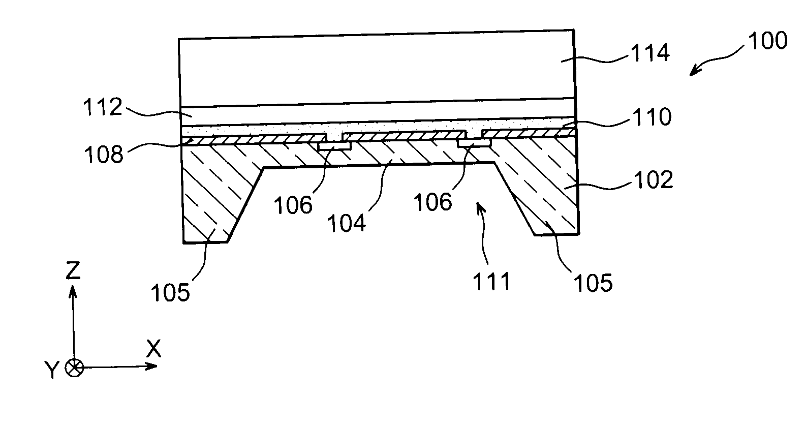
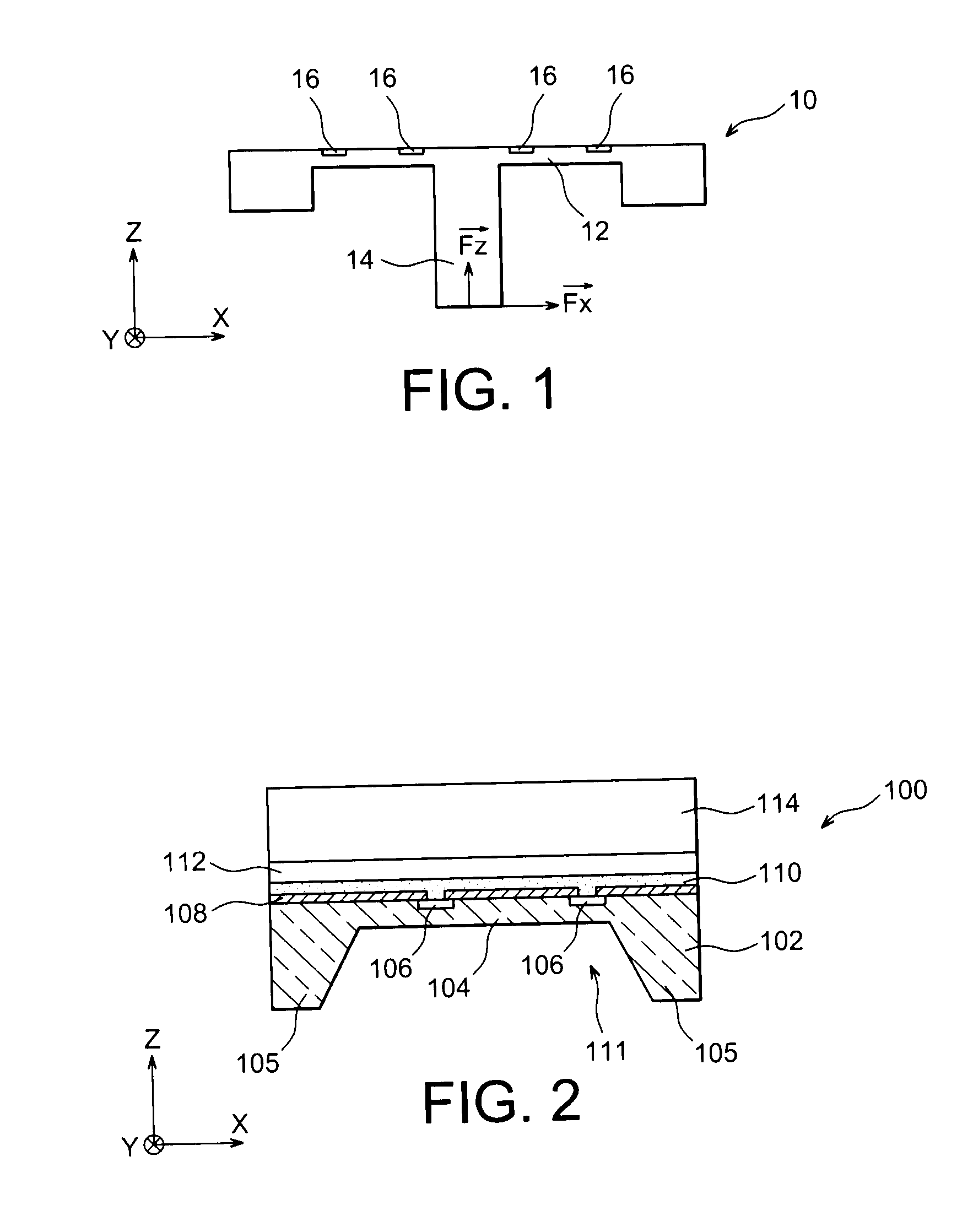
[0071]Reference is made first of all to FIG. 2, which shows a force sensor 100 according to a
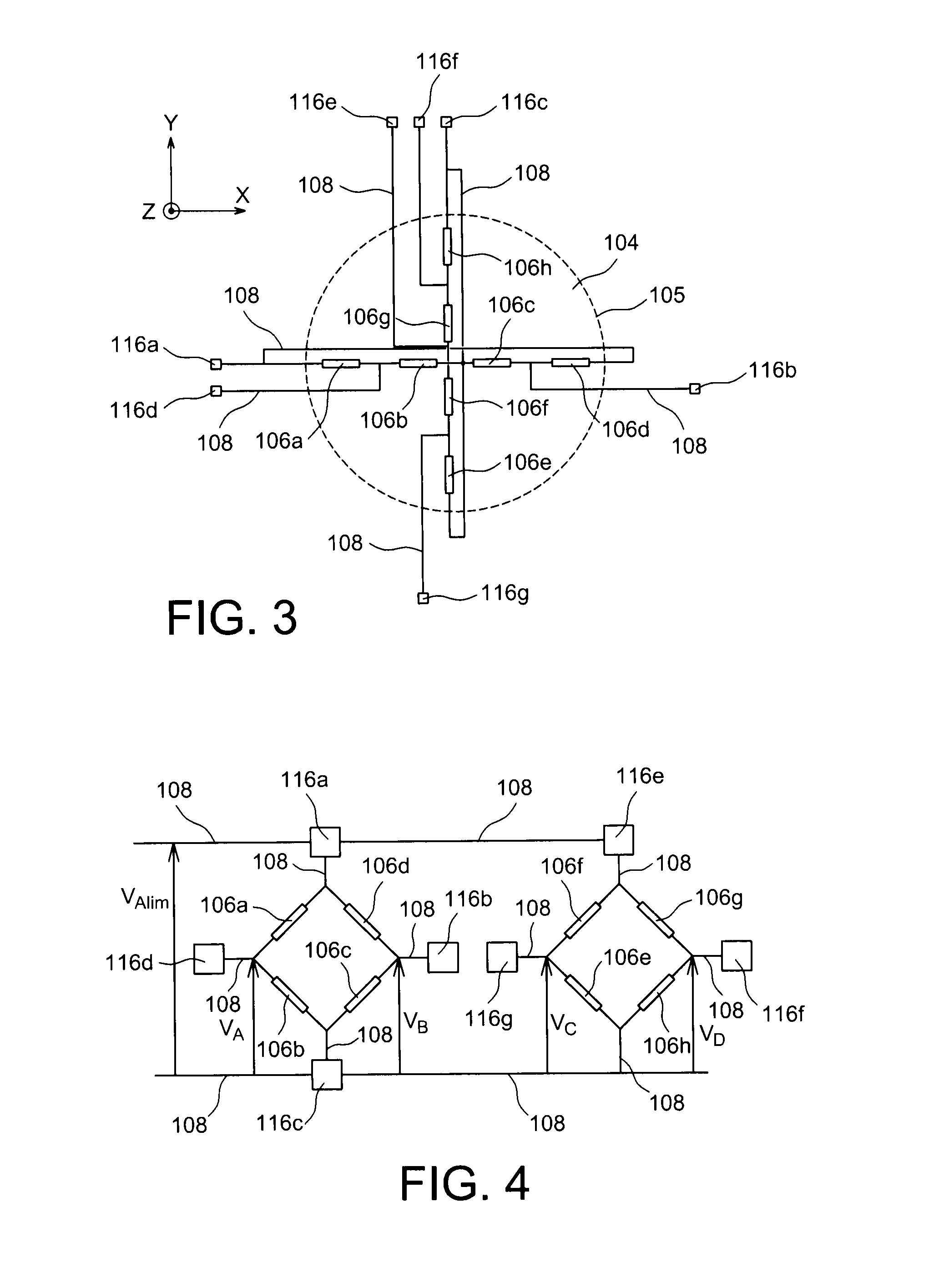
[0072]This sensor 100 is produced from a substrate 102, for example composed of a semiconductor such as silicon. The sensor 100 comprises a deformable membrane 104 comprising a portion of the substrate 102 etched over part of the thickness of the substrate 102. The deformable membrane 104 is here substantially flat, these dimensions in the plane of the substrate 102, that is to say in a plane parallel to the plane (X, Y) shown in FIG. 2, being very much greater than the thickness of the membrane 104 (dimension along the axis Z perpendicular to the plane of the substrate 102). The membrane 104 comprises two principal faces parallel to the plane of the substrate 102. Non-etched portions 105 of the substrate 102 form peripheral anchoring zones of the membrane 102. In this first embodiment, the form of the membrane 104 in the plane of the substrate 102 is a disc. However, the membrane 104 may ha...
second embodiment
[0081]Reference is now made to FIG. 5, which shows a force sensor 200 according to a
[0082]Compared with the sensor 100 previously described, the sensor 200 is not produced from a substrate of the bulk (solid) type but from an SOI (semiconductor on insulator) substrate comprising a solid layer 202, for example composed of a semiconductor such as silicon, on which are disposed a dielectric layer 204, for example composed of SiO2, and an active layer 206, here also composed of silicon.
[0083]The sensor 200 comprises a membrane 208 formed by a portion of the active layer 206 disposed on top of a cavity 210 formed in the dielectric sublayer 204. The membrane 208 has for example a form, in the plane of the substrate parallel to the plane (X, Y), similar to that of the membrane 104 previously described, that is to say a disc. The portions of the active layer 206 peripheral to the membrane 208 form peripheral anchoring regions for the membrane 208.
[0084]In a similar manner to the sensor 100,...
PUM
 Abstract
Description
Claims
Application Information
 - R&D Engineer
- R&D Manager
- IP Professional
- Industry Leading Data Capabilities
- Powerful AI technology
- Patent DNA Extraction
Browse by: Latest US Patents, China's latest patents, Technical Efficacy Thesaurus, Application Domain, Technology Topic.
© 2024 PatSnap. All rights reserved.Legal|Privacy policy|Modern Slavery Act Transparency Statement|Sitemap