Solid-state imaging element and electronic information device
a technology of solid-state imaging and electronic information, which is applied in the direction of semiconductor devices, basic electric elements, electrical appliances, etc., can solve the problems of increasing light, mixing colors, and worsening color reproducibility, so as to reduce the area of pixels, reduce color reproducibility, and increase the number of pixels
- Summary
- Abstract
- Description
- Claims
- Application Information
AI Technical Summary
Benefits of technology
Problems solved by technology
Method used
Image

Examples
embodiment 1
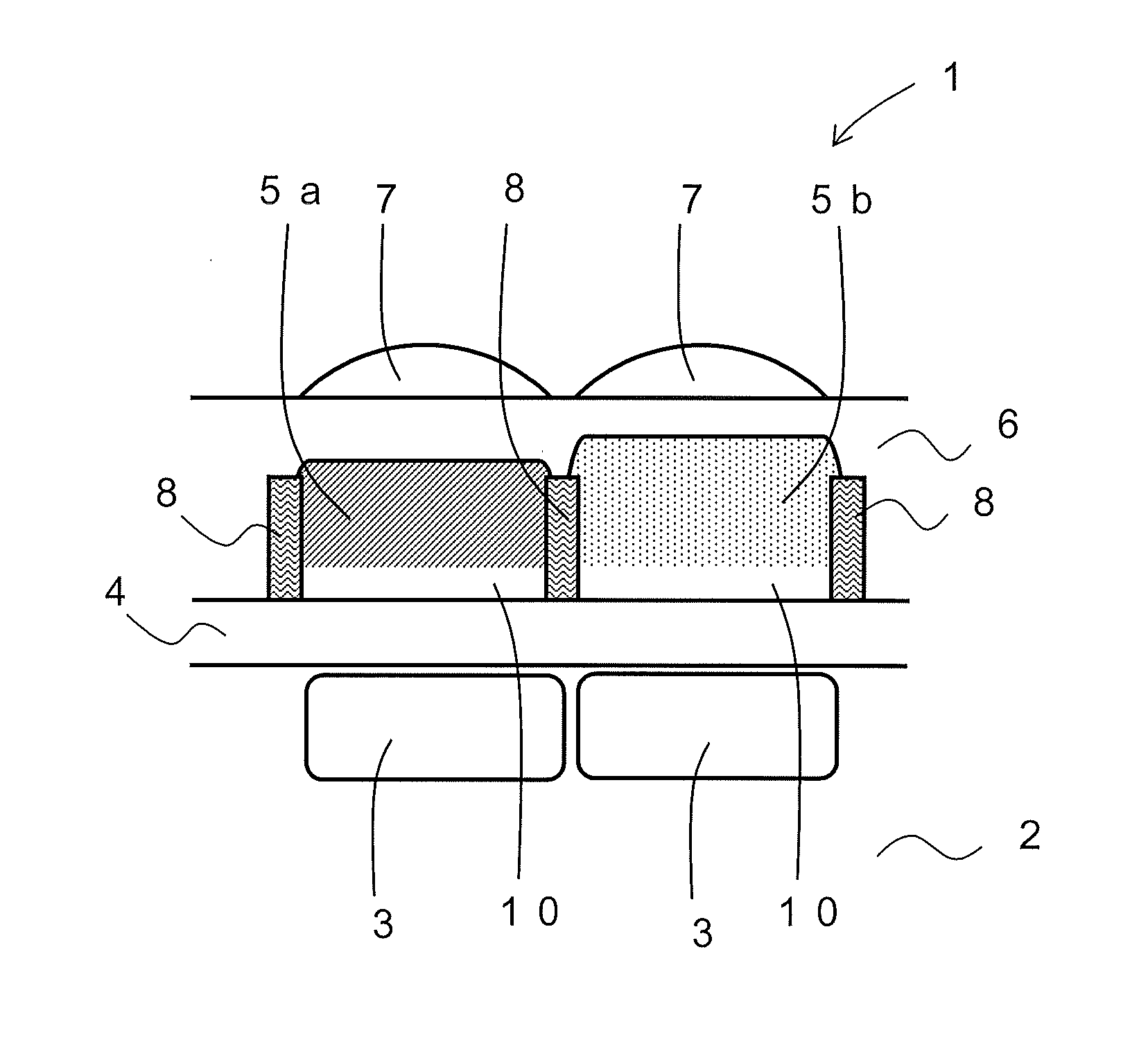
[0088]FIG. 1 is a longitudinal cross sectional view showing an example of an essential part structure of a solid-state imaging element according to Embodiment 1 of the present invention.
[0089]As shown in FIG. 1, a solid-state imaging element 1 according to Embodiment 1 includes a plurality of light receiving sections 3 arranged in a matrix in the upper part of a semiconductor substrate 2, the light receiving section 3 constituted of a semiconductor element for performing a photoelectric conversion on and capturing an image of image light from a subject. A color filter 5a or 5b is provided above each light receiving section 3, corresponding to each light receiving section 3, with a planarization film 4 and further a transparent film 10 (SiO2 film) interposed therebetween. A microlens 7 is provided above each color filter 5a or 5b, corresponding to each light receiving section 3, with a planarization film 6 interposed therebetween. The microlens 7 focuses incident light onto each ligh...
embodiment 2
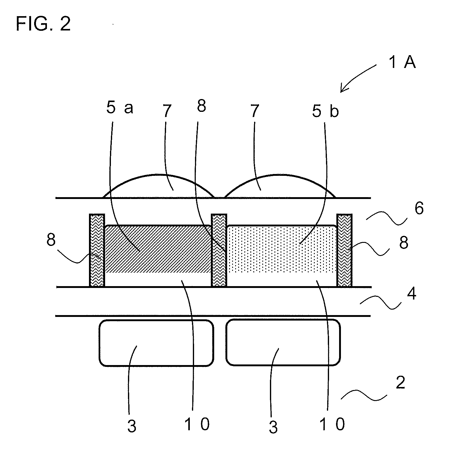
[0097]In Embodiment 2, a case will be described in which a transparent joining film is provided in between light shielding walls 8 (or reflection walls) and a color filter 5a or 5b embedded therebetween, for joining them (e.g., metal and an organic film).
[0098]FIG. 4 is a longitudinal cross sectional view showing an example of an essential part structure of a solid-state imaging element according to Embodiment 2 of the present invention. FIG. 4(a) is a longitudinal cross sectional view showing a case where a joining film is discontinuous. FIG. 4(b) is a longitudinal cross sectional view showing a case where a joining film is continuous.
[0099]As shown in FIG. 4(a), a solid-state imaging element 11 according to Embodiment 2 includes a plurality of light receiving sections 3 arranged in a matrix in the upper part of a semiconductor substrate 2, the light receiving section 3 constituted of a semiconductor element for performing a photoelectric conversion on and capturing an image of ima...
embodiment 3
[0105]In Embodiment 3, a case will be described where a light shielding wall 8 (or reflection wall) and / or a color filter 5a or 5b are provided directly on a semiconductor substrate 2.
[0106]FIG. 5 is a longitudinal cross sectional view showing an example of an essential part structure of a solid-state imaging element according to Embodiment 3 of the present invention.
[0107]As shown in FIG. 5, a solid-state imaging element 12 according to Embodiment 3 includes a plurality of light receiving sections 3 arranged in a matrix in the upper part of a semiconductor substrate 2, the light receiving section 3 constituted of a semiconductor element for performing a photoelectric conversion on and capturing an image of image light from a subject. The light receiving sections 3 are formed in the semiconductor substrate 2, and a color filter 5a or 5b is provided directly on the semiconductor substrate 2 (without a planarization film 4 interposed therebetween), corresponding to each light receivin...
PUM
 Abstract
Description
Claims
Application Information
 - R&D
- Intellectual Property
- Life Sciences
- Materials
- Tech Scout
- Unparalleled Data Quality
- Higher Quality Content
- 60% Fewer Hallucinations
Browse by: Latest US Patents, China's latest patents, Technical Efficacy Thesaurus, Application Domain, Technology Topic, Popular Technical Reports.
© 2025 PatSnap. All rights reserved.Legal|Privacy policy|Modern Slavery Act Transparency Statement|Sitemap|About US| Contact US: help@patsnap.com