Method for manufacturing a monolithic LED micro-display on an active matrix panel using flip-chip technology and display apparatus having the monolithic LED micro-display

Active Publication Date: 2011-12-22
NANO & ADVANCED MATERIALS INST
View PDF5 Cites 107 Cited by
  • Summary
  • Abstract
  • Description
  • Claims
  • Application Information

AI Technical Summary

Benefits of technology

[0010]According to an aspect, the subject matter is directed to a method for manufacturing a monolithic Light Emitting Diode (LED) micro-display panel on an Active Matrix (AM) panel, comprising: providing a substrate of the LED micro-display panel; providing a plurality of overlaying layers of material on a surface of the substrate, the plurality of overlaying layers of material being configured in combination to emit light when activated; patterning the plurality of overlaying layers of material by removing a part thereof all the way down to the surface of the substrate; depositing a current spreading layer on the plurality of overlaying layers of material and the surface of the substrate; providing a metal multilayer on the patterned plurality of overlaying layers of material and the surface of the substrate; patterning the metal multilayer in such a configuration that a first portion of the metal multilayer, which lies on the patterned plurality of overlaying layers of material, and a second portion of the metal multilayer, which lies on the surface of the substrate are conductively disconnected, thereby forming an micro-array of multiple monolithic LEDs; and combining the monolithic LED micro-display panel with the AM panel, which includes a plurality of active control circuit chips fixed thereon, the plurality of active control circuit chips being provided with conductive solder material thereon, in such a configuration that the monolithic LEDs are flip-chip bonded to the active control circuit chips via the conductive solder material and each

Problems solved by technology

The array dimensions and pixel brightness in conventional passively-addressable LED arrays were limited by the loading effect in the same row or column.
But the circuitry layer formed on the insulating layer can only be a thin film device like a-Si TFT or poly-Si TFT, however, these have low field effect mobility and cannot provide enough current for the LEDs.
On the other hand, these three patents adopt a bottom-emitting configuration and the aperture of the array is limited by the circuitry a

Method used


Image

  • Method for manufacturing a monolithic LED micro-display on an active matrix panel using flip-chip technology and display apparatus having the monolithic LED micro-display
  • Method for manufacturing a monolithic LED micro-display on an active matrix panel using flip-chip technology and display apparatus having the monolithic LED micro-display
  • Method for manufacturing a monolithic LED micro-display on an active matrix panel using flip-chip technology and display apparatus having the monolithic LED micro-display

Examples


Embodiment Construction

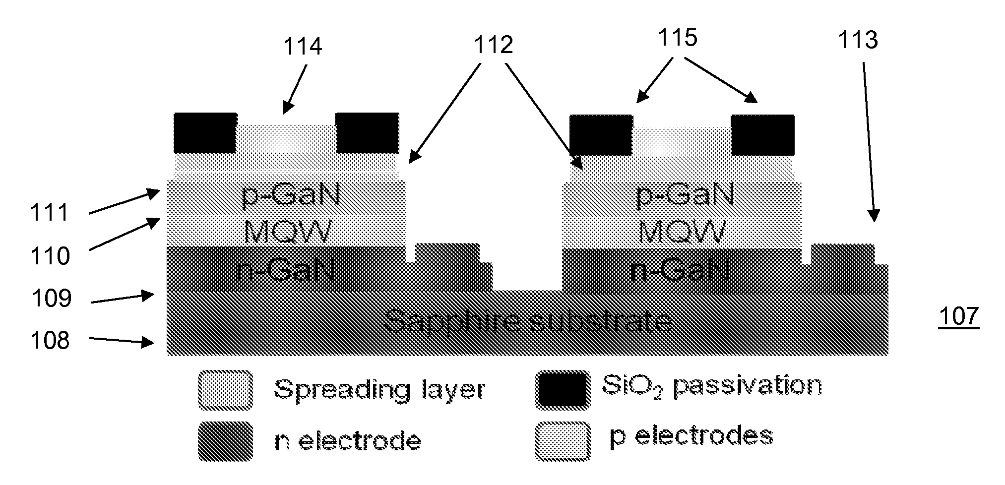
[0027]The Figures are diagrammatic and not drawn to scale. In the Figures, elements which correspond to elements already described have the same reference numerals.

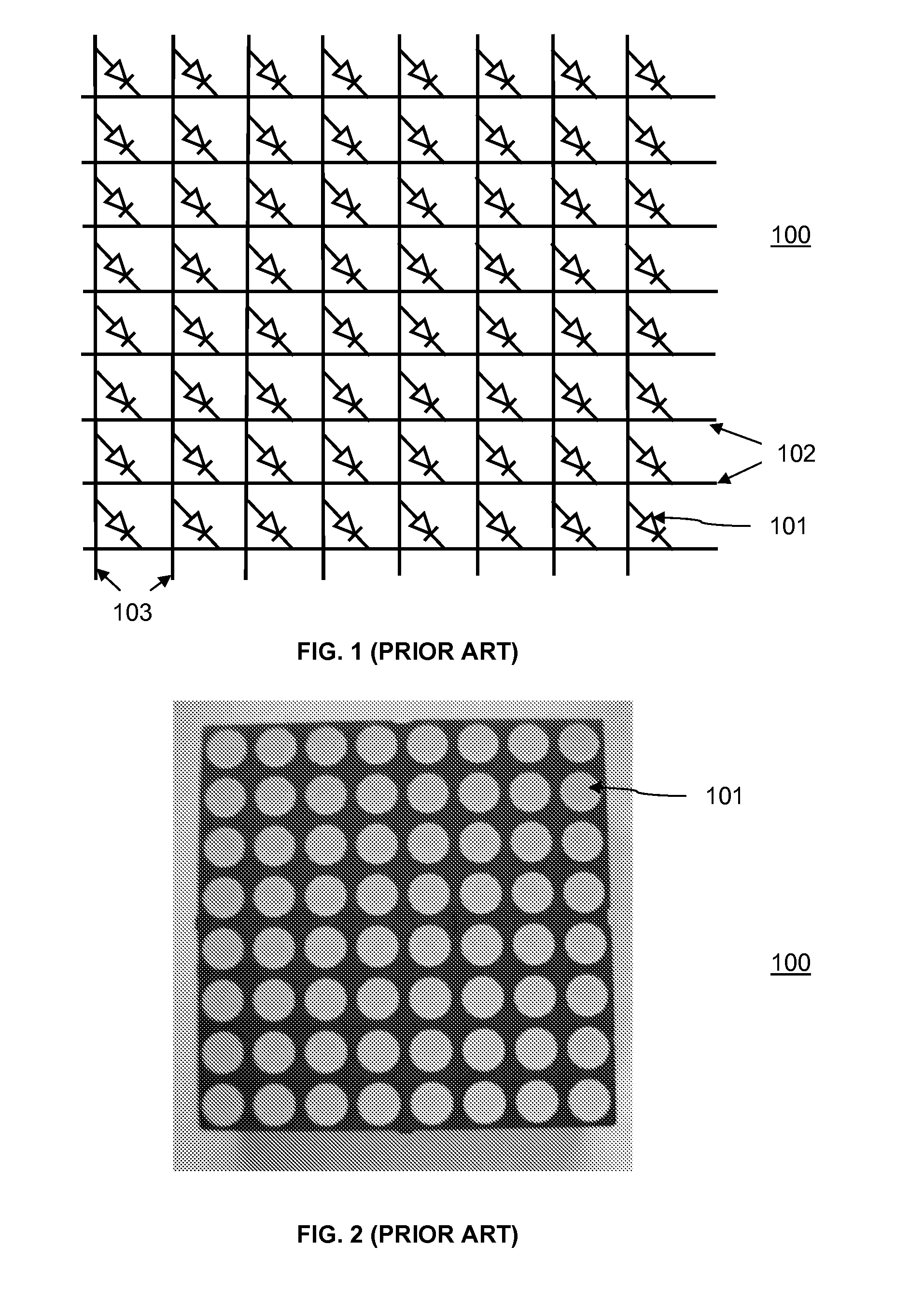
[0028]FIG. 1 is a simplified schematic diagram of a top plan view of a prior art passive LED matrix 100 wherein the passive LED matrix 100 includes a plurality of LEDs 101 arranged in rows and columns with anodes in a same column connected to one another via column buses 102 and cathodes in a same column connected to one another via row buses 103. FIG. 2 shows a top plan view of the prior art passive LED matrix, as schematically shown in FIG. 1.

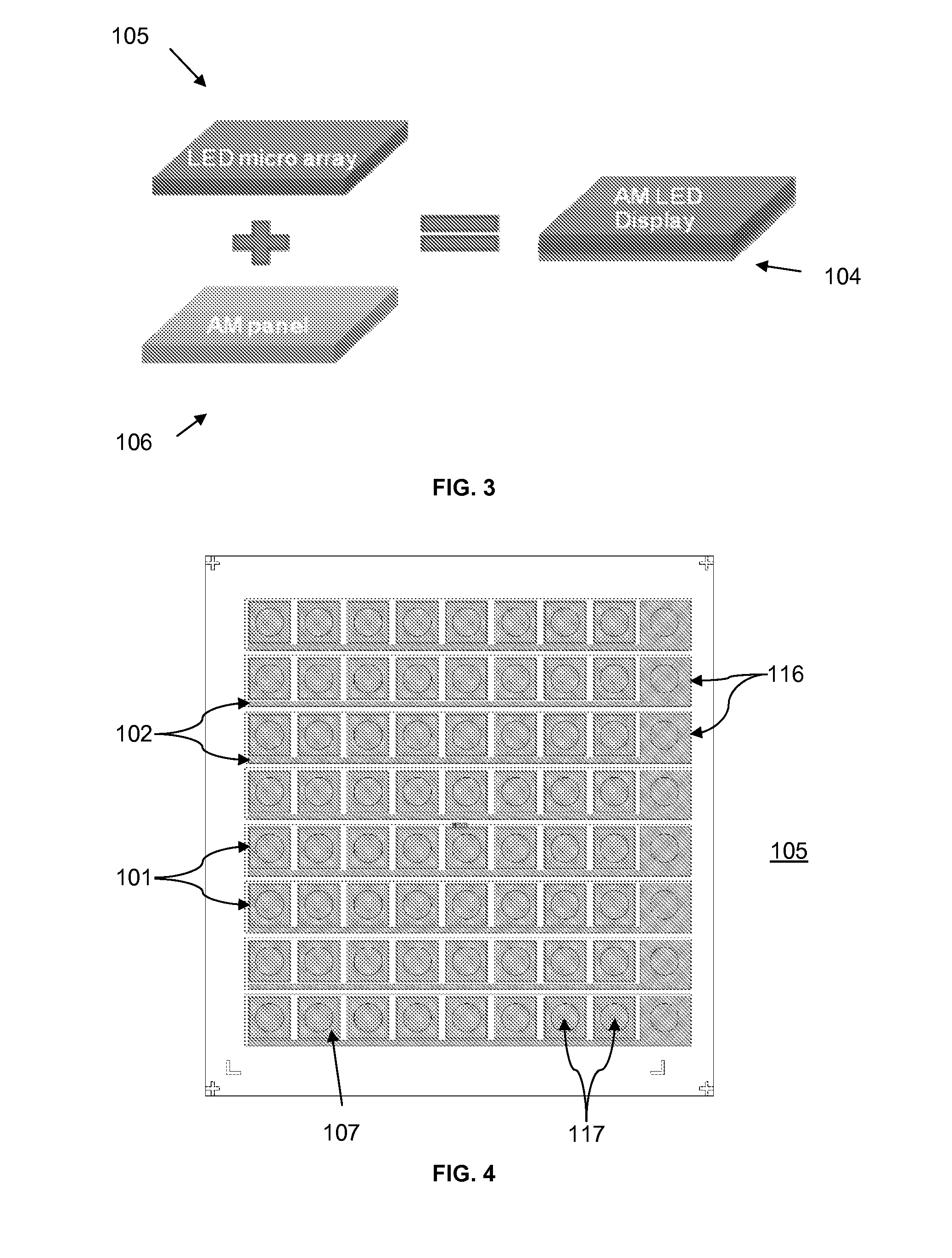
[0029]FIG. 3 schematically shows a manufacture of an AM LED display 104 according to the present subject matter by flip-chip boding an LED micro-array panel 105 with an AM panel 106. The flip-chip bonding is a method for interconnecting semiconductor devices, such as Integrated Circuit (IC) chips and micro-electromechanical systems, to external circuitry with solder bumps that have...


PUM


Abstract

A high-resolution, Active Matrix (AM) programmed monolithic Light Emitting Diode (LED) micro-array is fabricated using flip-chip technology. The fabrication process includes fabrications of an LED micro-array and an AM panel, and combining the resulting LED micro-array and AM panel using the flip-chip technology. The LED micro-array is grown and fabricated on a sapphire substrate and the AM panel can be fabricated using CMOS process. LED pixels in a same row share a common N-bus line that is connected to the ground of AM panel while p-electrodes of the LED pixels are electrically separated such that each p-electrode is independently connected to an output of drive circuits mounted on the AM panel. The LED micro-array is flip-chip bonded to the AM panel so that the AM panel controls the LED pixels individually and the LED pixels exhibit excellent emission uniformity. According to this constitution, incompatibility between the LED process and the CMOS process can be eliminated.

Description

BACKGROUND OF THE INVENTION[0001]1. Field of the Invention[0002]The present subject matter relates generally to manufacturing a Light Emitting Diode (LED) micro-display on an Active Matrix (AM) panel, and more specifically to manufacturing an LED micro-display on an AM panel using flip-chip technology.[0003]2. Related Art[0004]LED array displays made with individually packaged devices have been widely used for various applications. In recent years, different techniques have been exploited to fabricate monolithic, passively-addressable LED arrays. The array dimensions and pixel brightness in conventional passively-addressable LED arrays were limited by the loading effect in the same row or column. Thus, various new address schemes and fabrication technologies are suggested to improve the operating effectiveness of monolithic LED arrays.[0005]For example, U.S. Pat. Nos. 5,789,766, 5,827,753, and 5,893,721 relate to methods of fabricating an LED array and driving circuitry that include...

Claims


Application Information

Patent Timeline
IPC IPC(8): H01L33/62
CPCH01L27/1214H01L27/1225H01L33/08H01L33/40H01L27/156
Inventor LAU, KEI MAYKEUNG, CHI WINGLIU, ZHAOJUN
Owner NANO & ADVANCED MATERIALS INST
Why Eureka
Try Eureka