Method for manufacturing substrate for light emitting element package, and light emitting element package

a technology of light emitting elements and manufacturing methods, applied in the directions of transportation and packaging, printed circuit aspects, chemistry apparatuses and processes, etc., can solve the problems of high processing cost, and achieve the effects of good heat conductivity, excellent mass productivity, and easy operation

Inactive Publication Date: 2011-12-22
DENKA CO LTD
View PDF0 Cites 14 Cited by
  • Summary
  • Abstract
  • Description
  • Claims
  • Application Information

AI Technical Summary

Benefits of technology

[0015]According to the method for manufacturing a substrate for a light emitting element package of the present invention, the laminate having an insulating adhesive agent with a good heat conductivity and a metal layer member can be laminated and integrated with the metal layer member having a thick metal section. By producing the laminate in advance, the production of the substrate for a light emitting element package can be easily carried out, thereby providing excellent mass productivity and enabling cost reduction and downsizing of the package. Further, for example, when the light emitting element is mounted on the metal layer surface side opposite to the thick metal section, the heat generated in the light emitting element is efficiently conducted by the thick metal section, and the heat is efficiently conducted further by the insulating layer having a high heat conductivity, whereby a sufficient heat dissipation effect can be obtained as a substrate for packaging.
[0016]Also, as one example of a suitable embodiment of the present invention, it is preferable that the laminate having the insulating adhesive agent and the metal layer member and / or the metal layer member having the thick metal section are provided in a roll form in advance. With this construction, the continuous production property and the mass production property will be excellent and also the yield efficiency will be good as compared with the production in sheet units.
[0017]Also, as one example of a suitable embodiment of the present invention, it is preferable that the thick metal section is laminated so that the thick metal section will be contained in the inside of the insulating layer of the laminate. With this construction, the top side of the thick metal section is buried in the insulating layer having a high heat conductivity (a state in which the insulating adhesive agent is cured; the same applies hereafter), thereby increasing the heat conduction area. Therefore, the heat from the thick metal section can be more efficiently conducted to the whole package.
[0018]Also, as one example of a suitable embodiment of the present invention, the method is characterized by having a removal step of removing the laminate so that the thick metal section will be exposed. With this construction, the top side of the thick metal section is exposed (a state in which the thick metal section penetrates through the insulating layer), and the light emitting element can be mounted directly or via an indirect layer such as a pad onto this top side of the thick metal section. In the case of such a structure, the light emitting element is mounted on the thick metal section side, so that the heat generated in the light emitting element is efficiently conducted. Furthermore, the heat is efficiently conducted to the insulating layer side via the thick metal section.
[0019]Also, as one example of a suitable embodiment of the present invention, it is preferable that the method further includes a step of winding and collecting in a roll form after the lamination step. With this construction, by winding and collecting the laminate (substrate member) having been subjected to the lamination step in a roll form, the laminate can be easily transported to the next step, and the laminate (substrate member) can be easily drawn out, for example, in the patterning step or in the cutting step. Also, the area for storage can be reduced.
[0020]Also, the light emitting element package of the present invention is constructed by using a substrate for a light emitting element package manufactured by the above-described manufacturing method. Therefore, the light emitting element package can be manufactured at a low cost and to have a small scale.

Problems solved by technology

However, with this substrate, the structure will be complex, raising problems such as a high processing cost.

Method used


Image

  • Method for manufacturing substrate for light emitting element package, and light emitting element package
  • Method for manufacturing substrate for light emitting element package, and light emitting element package
  • Method for manufacturing substrate for light emitting element package, and light emitting element package

Examples


Embodiment Construction

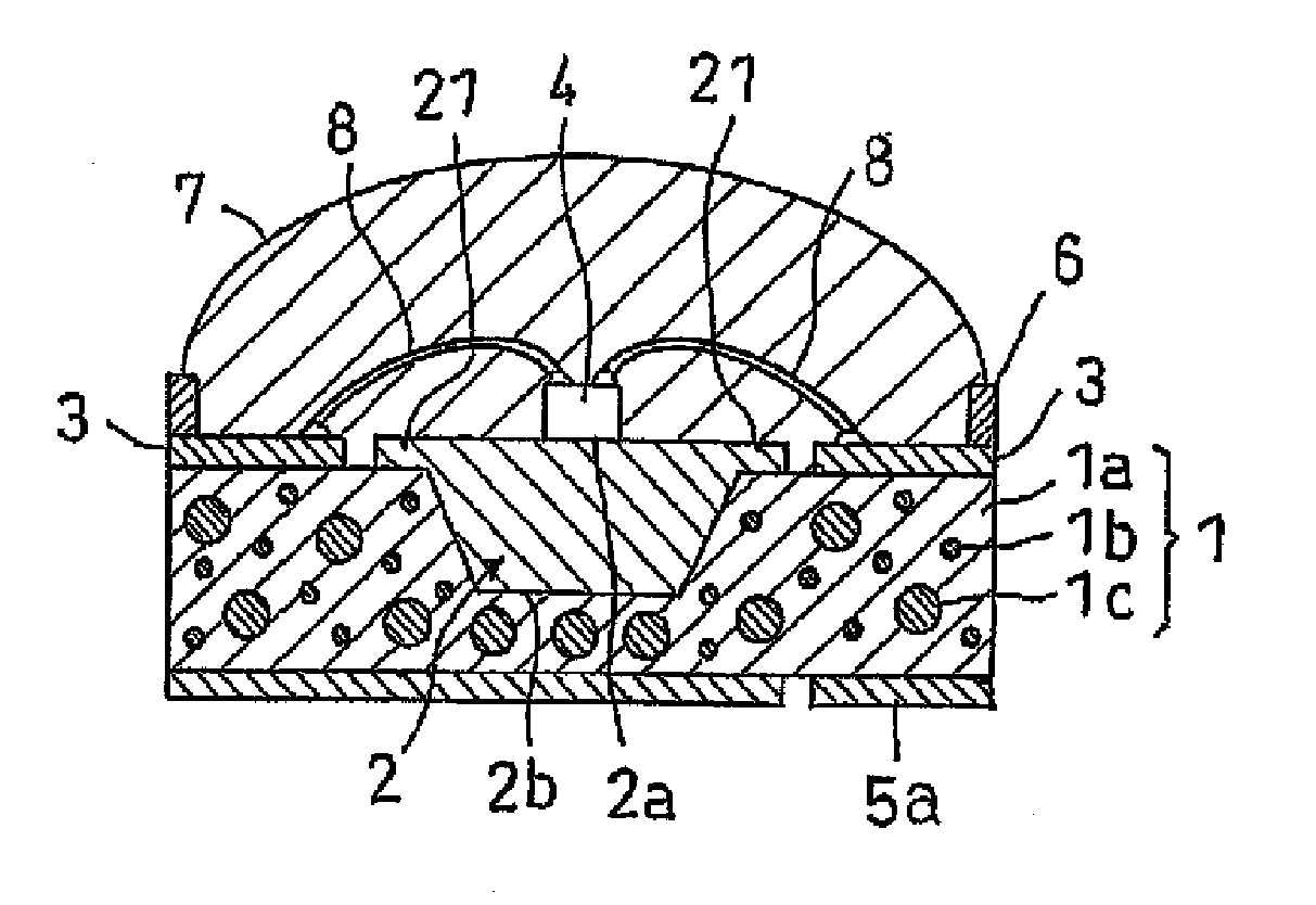
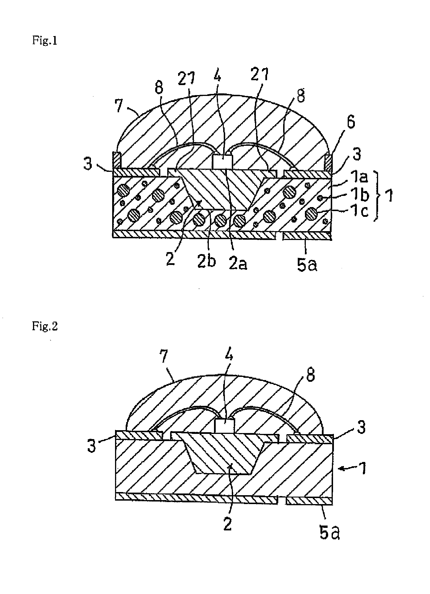
[0043]Hereafter, embodiments of the present invention will be described with reference to the drawings. FIG. 1 is a cross-sectional view showing one example of a substrate for a light emitting element package of the present invention, showing a state in which a light emitting element is mounted and packaged.

[0044]Referring to FIG. 1, the substrate for a light emitting element package of the present invention includes an insulating layer 1 composed of a resin 1a containing heat conductive fillers 1b, 1c, a metal layer 21 disposed under a mounting position of a light emitting element 4 and provided with a thick metal section 2, and a surface electrode section 3 formed on a mounting side surface of the insulating layer 1.

[0045]In the present embodiment, the light emitting element 4 is mounted directly on the mounting surface 2a of the metal layer 21. The thick metal section 2 is formed to be thick from the mounting surface 2a towards a back side of the insulating layer 1, and the top s...


PUM

PropertyMeasurementUnit
median diameteraaaaaaaaaa
diameteraaaaaaaaaa

Abstract

A method for manufacturing a substrate for a light emitting element package provided with a thick metal section formed under a mounting position of a light emitting element, having a lamination step of laminating and integrating a laminate having an insulating adhesive agent which is composed of a resin containing heat conductive fillers and has a heat conductivity of 1.0 W/mK or more and a metal layer member, with a metal layer member having a thick metal section while drawing out each member.

Description

TECHNICAL FIELD[0001]The present invention relates to a method for manufacturing a substrate for a light emitting element package used in packaging a light emitting element such as a LED chip, as well as to a light emitting element package using a substrate for a light emitting element package manufactured by this manufacturing method.BACKGROUND ART[0002]In recent years, as illuminating and light-emitting means that can reduce the weight and thickness and can save electric power consumption, a light emitting diode has been attracting people's attention. As a mode of mounting a light emitting diode, there are known a method of mounting a bare chip (LED chip) of a light emitting diode directly on a circuit board and a method of packaging a LED chip by bonding on a small substrate so that the LED chip can be easily mounted on the circuit board and mounting this LED package on the circuit board.[0003]A conventional LED package has a structure such that a LED chip is die-bonded onto a sm...

Claims


Application Information

Patent Timeline
Patent Type & Authority Applications(United States)
IPC IPC(8): B32B15/08B32B37/12
CPCH01L33/486H01L33/641H05K2203/1545H01L33/642H01L2224/32188H01L2224/48091H01L2924/01004H01L2924/01012H01L2924/01046H01L2924/01057H01L2924/01078H01L2924/01079H05K1/0204H05K1/0206H05K1/056H05K3/022H05K2201/0209H05K2201/09054H05K2201/09736H05K2201/10106H01L2924/00014Y10T428/31678H01L33/48H01L33/02
Inventor SUZUKI, MOTOHIROYONEMURA, NAOMIOKAJIMA, YOSHIHIKOMAEDA, TETSUROYOSHIMURA, EIJI
Owner DENKA CO LTD
Why Eureka
Try Eureka