Schottky junction si nanowire field-effect bio-sensor/molecule detector
- Summary
- Abstract
- Description
- Claims
- Application Information
AI Technical Summary
Benefits of technology
Problems solved by technology
Method used
Image
Examples
Embodiment Construction
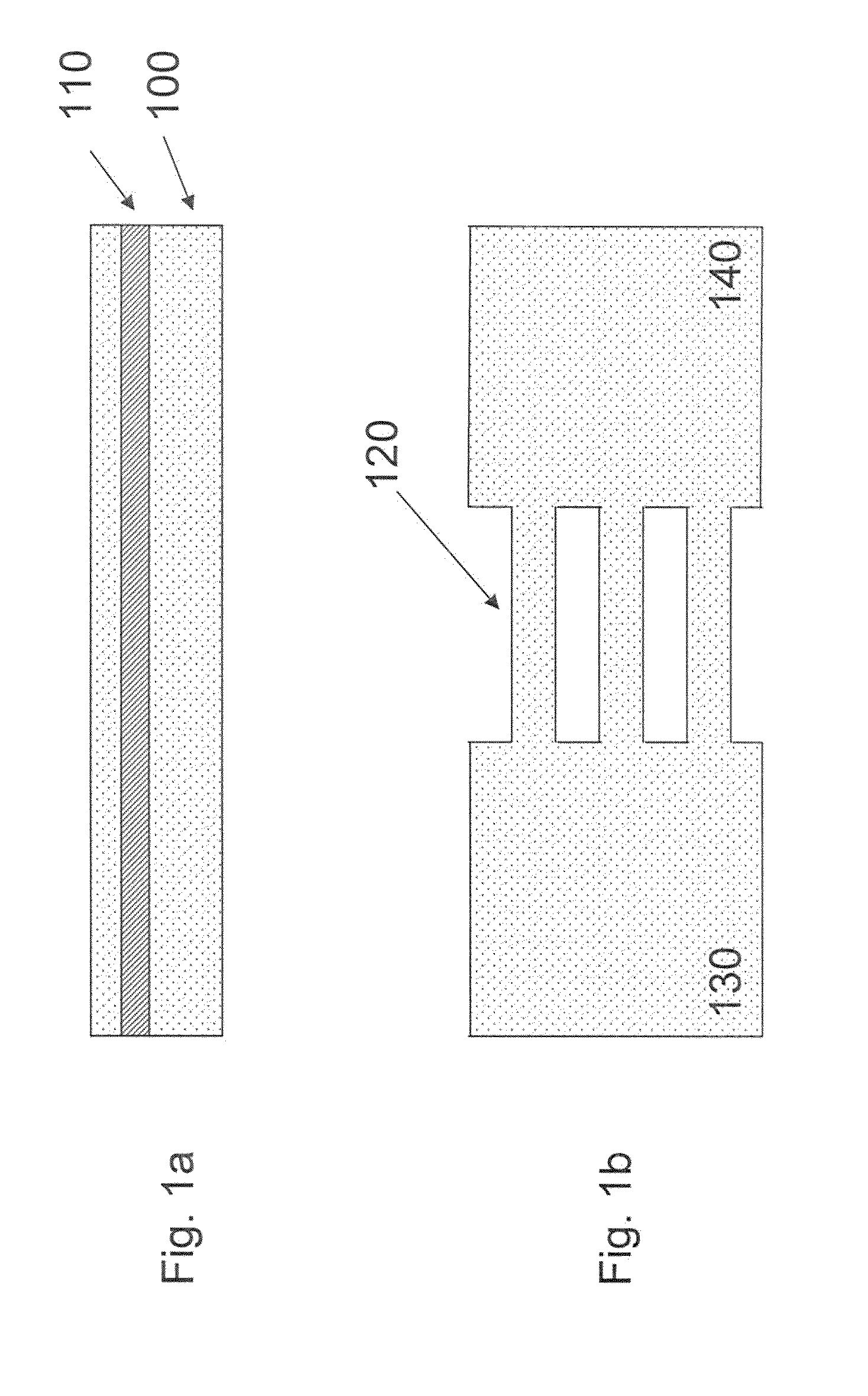
[0018]Turning to the drawings. FIGS. 1a and 1b show an early processing step in the formation of Schottky junction field-effect sensor with a nanowire 120 being formed between two electrodes 130 and 140. As described in detail below, the nanowire 120 will form the channel region of the Schottky junction field-effect sensor. In this particular embodiment, three nanowires are formed between the electrodes, but the number of nanowires is not particularly limited as structures including one, two or more than three nanowires are also within the scope of this disclosure. The structure of a nanowire and two electrodes is typically formed by a lithographic process. Also typically, substrate 100 in FIG. 1a is silicon.
[0019]With particularity, the imbedded dielectric layer 110 shown in FIG. 1a is silicon dioxide, but other dielectric materials may also be used.
[0020]Typically, the channel region of the Schottky junction field-effect sensor has a thickness of 10 nanometers or less. With partic...
PUM
 Abstract
Description
Claims
Application Information


