

Signal processing circuit and antenna apparatus
- Summary
- Abstract
- Description
- Claims
- Application Information
AI Technical Summary
Benefits of technology
Problems solved by technology
Method used
Image

Examples
first preferred embodiment
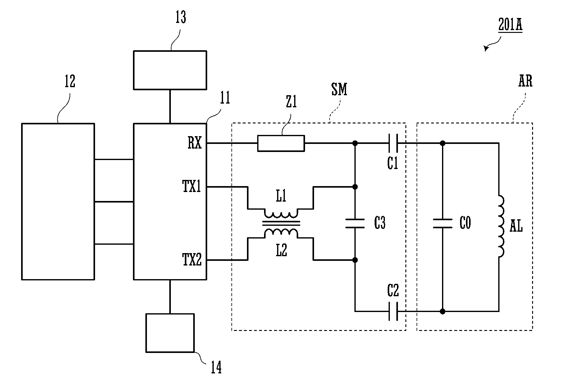
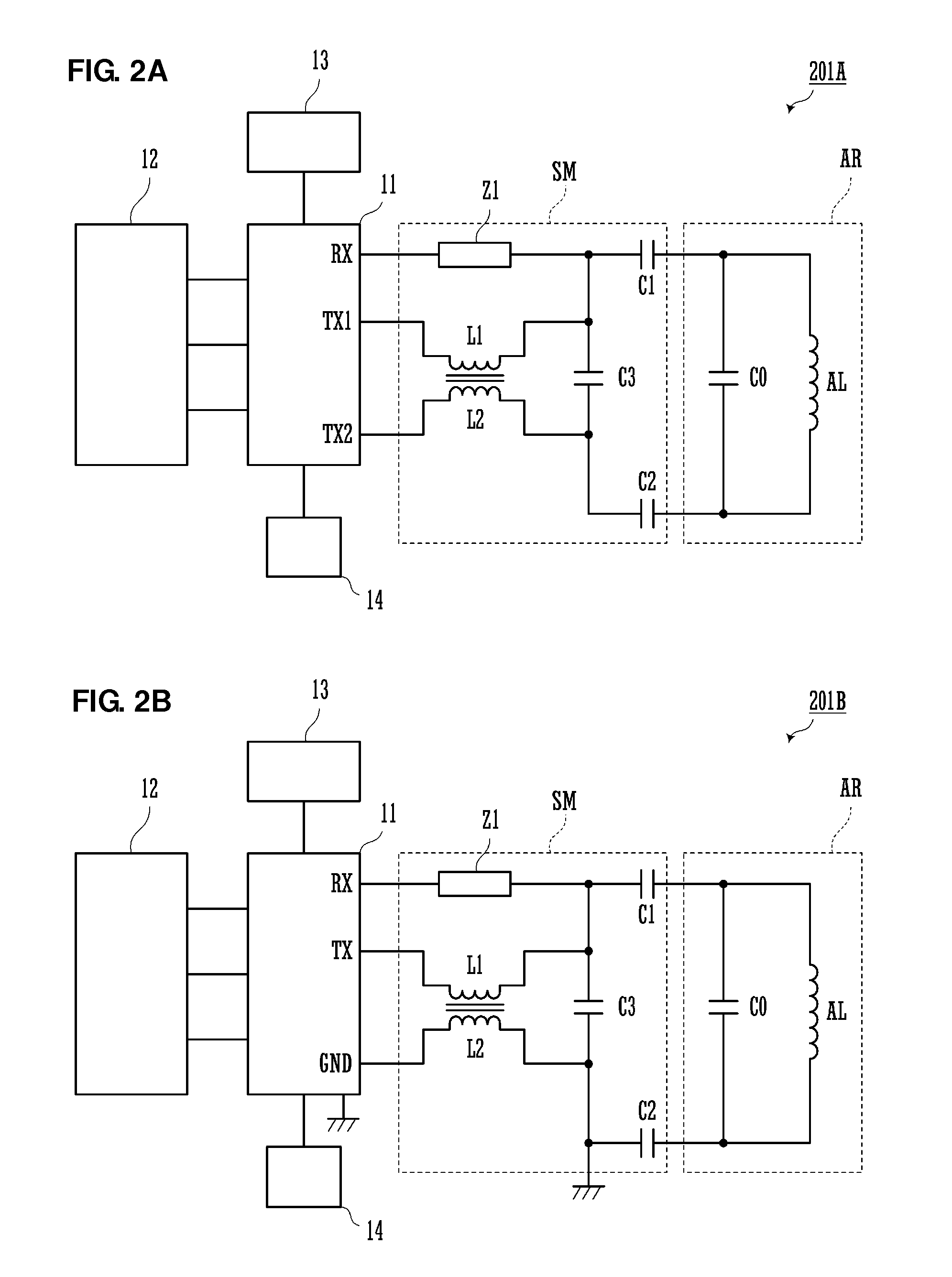
[0033]FIG. 2A is a circuit diagram of a wireless IC device 201A according to a first preferred embodiment of the present invention. FIG. 2B is a circuit diagram of another wireless IC device, 201B, according to the first preferred embodiment of the present invention.
[0034]First, FIG. 2A will be described. As shown in FIG. 2A, an antenna coil AL and a capacitor CO define an antenna resonant circuit AR.
[0035]The wireless IC device 201A includes the antenna resonant circuit AR, a wireless IC 11, a control unit 12, a cipher processing unit 13, and a clock circuit 14. A characteristic stabilization circuit SM to perform impedance matching is preferably provided between the antenna resonant circuit AR and the wireless IC 11. The characteristic stabilization circuit SM corresponds to a “signal processing circuit” according to a preferred embodiment of the present invention. Specifically, a series circuit of capacitors C1, C2, and C3 is connected in parallel with the antenna resonant circui...
second preferred embodiment
[0049]FIG. 5 is a sectional view of the main portion of a wireless IC device 202 according to a second preferred embodiment. FIG. 6 is a drawing showing the configuration of two coils, L1 and L2, provided within the wireless IC device 202. The circuit configuration of the wireless IC device is similar to that according to the first preferred embodiment shown in FIG. 2.
[0050]In the example shown in FIG. 6, the two coils, L1 and L2, are preferably arranged to have a spiral configuration, for example. The first coil L1 is disposed inside the second coil L2 on approximately the same plane. A port #1 is connected to an antenna resonant circuit AR side, and a second port #2 is connected to a wireless IC side. The disposition of one coil, L1, inside the other coil, L2, as described above can strengthen the coupling between the two coils, L1 and L2, reliably matching impedances.
[0051]As shown in FIG. 5, the two coils, L1 and L2, shown in FIG. 5 are preferably provided in approximately the s...
third preferred embodiment
[0053]FIG. 7A is a circuit diagram of a wireless IC device 203A according to a third preferred embodiment of the present invention. FIG. 7B is a circuit diagram of another wireless IC device, 203B, according to the third preferred embodiment of the present invention.
[0054]First, FIG. 7A will be described. As shown in FIG. 7A, the wireless IC device 203A includes an antenna resonant circuit AR, a wireless IC 11, a control unit 12, a cipher processing unit 13, a clock circuit 14, and a characteristic stabilization circuit SM to match impedances between the wireless IC 11 and the antenna resonant circuit AR. The characteristic stabilization circuit SM has a configuration different from that according to the first preferred embodiment shown in FIG. 2. Another difference is that the wireless IC 11 includes receiving terminals RX1 and RX2, which are balanced inputs.
[0055]Both end portions of a first coil L11 are connected to the two receiving terminals, RX1 and RX2, of the wireless IC 11....
PUM
 Abstract
Description
Claims
Application Information