Semiconductor device having semiconductor substrate including diode region and IGBT region

a semiconductor substrate and semiconductor technology, applied in semiconductor devices, diodes, electrical devices, etc., can solve the problem of large manufacturing error range in which charged particles are implanted, and achieve the effect of easy recombin

Active Publication Date: 2012-01-12
DENSO CORP
View PDF3 Cites 30 Cited by
  • Summary
  • Abstract
  • Description
  • Claims
  • Application Information

AI Technical Summary

Benefits of technology

[0007]The diode lifetime control region is a region wherein a carrier lifetime is shortened, and includes, for example, a region where crystal defects are formed by implanting charged particles. By forming the diode lifetime control region within the diode drift region, carriers in the diode drift region can be more easily recombined and dissipated when the diode performs the reverse recovery. Consequently, the reverse current that flows when the diode performs the reverse recovery can be suppressed. According to this semiconductor device, the end of the diode lifetime control region on the IGBT region side is located right below the separation region, therefore even if the position of the end varies, an area of the diode lifetime control region within the diode region does not change. Consequently, in a case of this semiconductor device, the reverse recovery characteristics of the diodes hardly vary.

Problems solved by technology

In a step of implanting charged particles, a manufacturing error of a range in which the charged particles are implanted is large.
In other words, in this semiconductor device, the characteristics of the diode and the characteristics of the IGBT easily vary due to the manufacturing error in a range where the damage layer is formed.

Method used


Image

  • Semiconductor device having semiconductor substrate including diode region and IGBT region
  • Semiconductor device having semiconductor substrate including diode region and IGBT region

Examples


Embodiment Construction

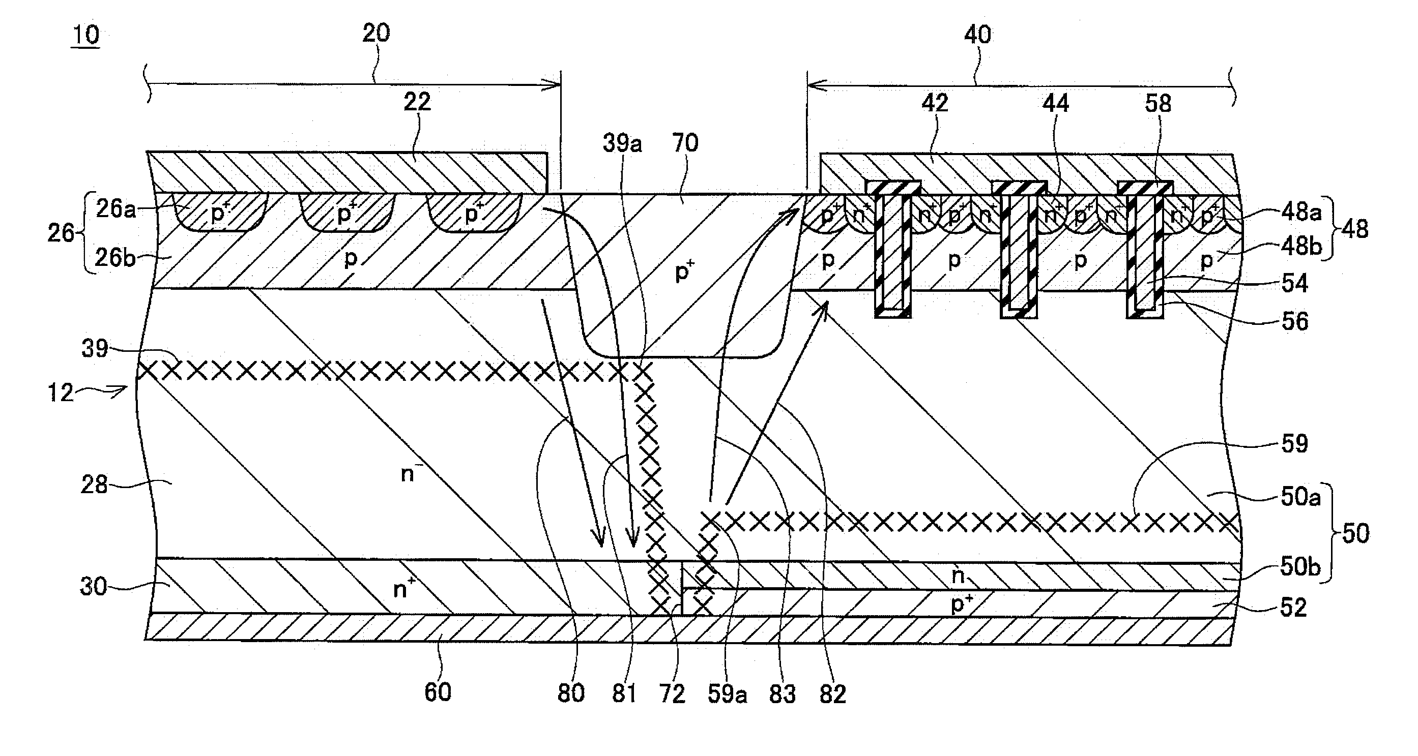
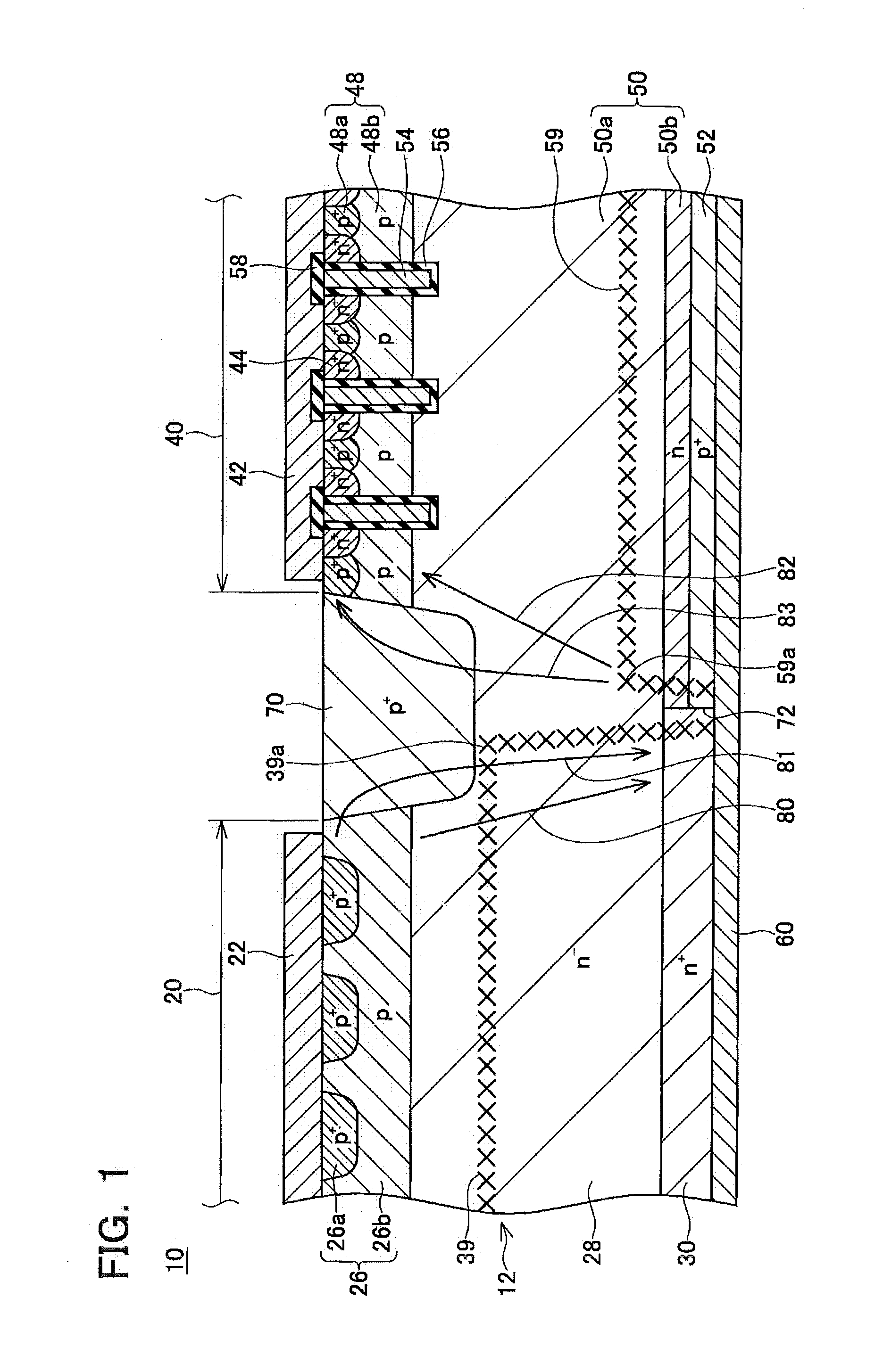
[0009]An embodiment of a semiconductor device of the present techings may preferably be configured as follows. An IGBT lifetime control region may be formed within a IGBT drift region. A carrier lifetime in the IGBT lifetime control region may be shorter than that in the IGBT drift region outside the IGBT lifetime control region. An end of the IGBT lifetime control region on a diode region side may be located right below a separation region. The IGBT lifetime control region is a region wherein a carrier lifetime is shortened, and includes, for example, a region where crystal defects are formed by implanting charged particles. By forming the IGBT lifetime control region within the IGBT drift region, carriers in the IGBT drift region can be more easily recombined and dissipated when the IGBT turns OFF. This makes it possible to improve the turn OFF speed of the IGBT. According to this semiconductor device, the end of the IGBT lifetime control region on the diode region side is located...


PUM


Abstract

Provided is a semiconductor device including a semiconductor substrate in which a diode region and an IGBT region are formed. A separation region formed of a p-type semiconductor is formed in a range between the diode region and the IGBT region and extending from an upper surface of the semiconductor substrate to a position deeper than both a lower end of an anode region and a lower end of a body region. A diode lifetime control region is formed within a diode drift region. A carrier lifetime in the diode lifetime control region is shorter than that in the diode drift region outside the diode lifetime control region. An end of the diode lifetime control region on an IGBT region side is located right below the separation region.

Description

CROSS-REFERENCE TO RELATED APPLICATION[0001]This application is a continuation of PCT application serial no. PCT / JP2009 / 065606 filed on Sep. 7, 2009, the disclosure of which is hereby incorporated by reference herein in its entirety.TECHNICAL FIELD[0002]The present teachings relate to a semiconductor device having a semiconductor substrate in which a diode region and an IGBT region are formed.DESCRIPTION OF RELATED ART[0003]Japanese Patent Application Laid-Open No. 2008-192737 discloses a semiconductor device having a semiconductor substrate in which a diode region and an IGBT region are formed. A damage layer is formed within the diode region. Since the damage layer becomes a center of recombining of carriers, reverse current that flows in the diode upon reverse recovery is decreased.BRIEF SUMMARY[0004]A damage layer is normally formed by implanting charged particles into a semiconductor substrate. In a step of implanting charged particles, a manufacturing error of a range in which...

Claims


Application Information

Patent Timeline
Patent Type & Authority Applications(United States)
IPC IPC(8): H01L27/06
CPCH01L21/761H01L27/0727H01L29/861H01L29/7397H01L29/32H01L27/0652
Inventor NAGAOKA, TATSUJISOENO, AKITAKA
Owner DENSO CORP
Why Eureka
Try Eureka