Method for producing photoelectric converter and photoelectric converter

Active Publication Date: 2015-01-01
KYOCERA CORP
View PDF8 Cites 0 Cited by
  • Summary
  • Abstract
  • Description
  • Claims
  • Application Information

AI Technical Summary

Benefits of technology

The method presented in this patent inhibits the release of hydrogen from the protective film on a substrate during heat application, which prevents carriers from recombining at the surface of the substrate and reduces the lifetime of carriers. This results in a higher current being extracted from the substrate. Additionally, the hydrogen concentration in the first protective film is higher than in the second protective film, which further reduces surface recombination.

Problems solved by technology

This makes it difficult to increase the current extracted from the substrate.

Method used


Image

  • Method for producing photoelectric converter and photoelectric converter
  • Method for producing photoelectric converter and photoelectric converter
  • Method for producing photoelectric converter and photoelectric converter

Examples


example 1

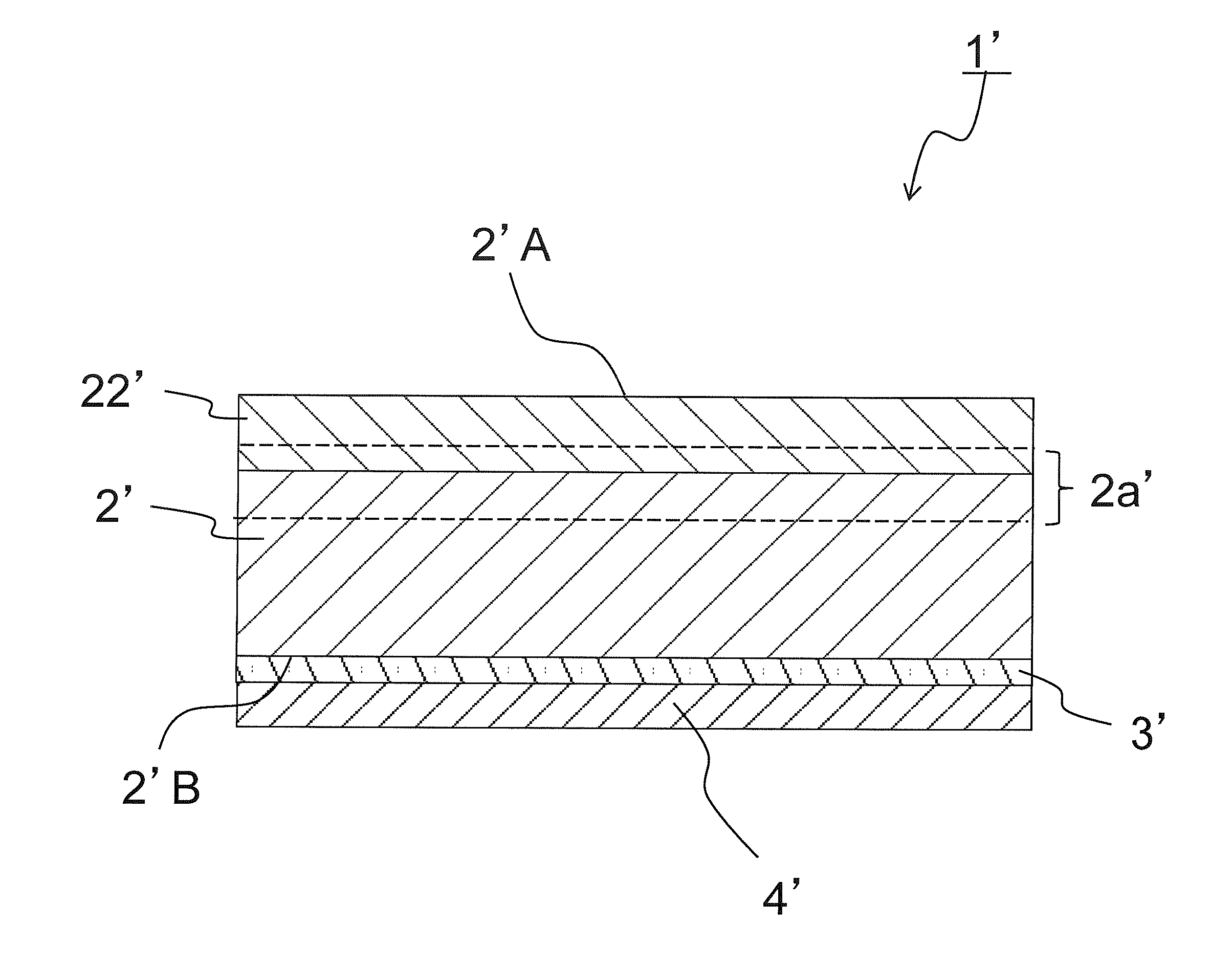
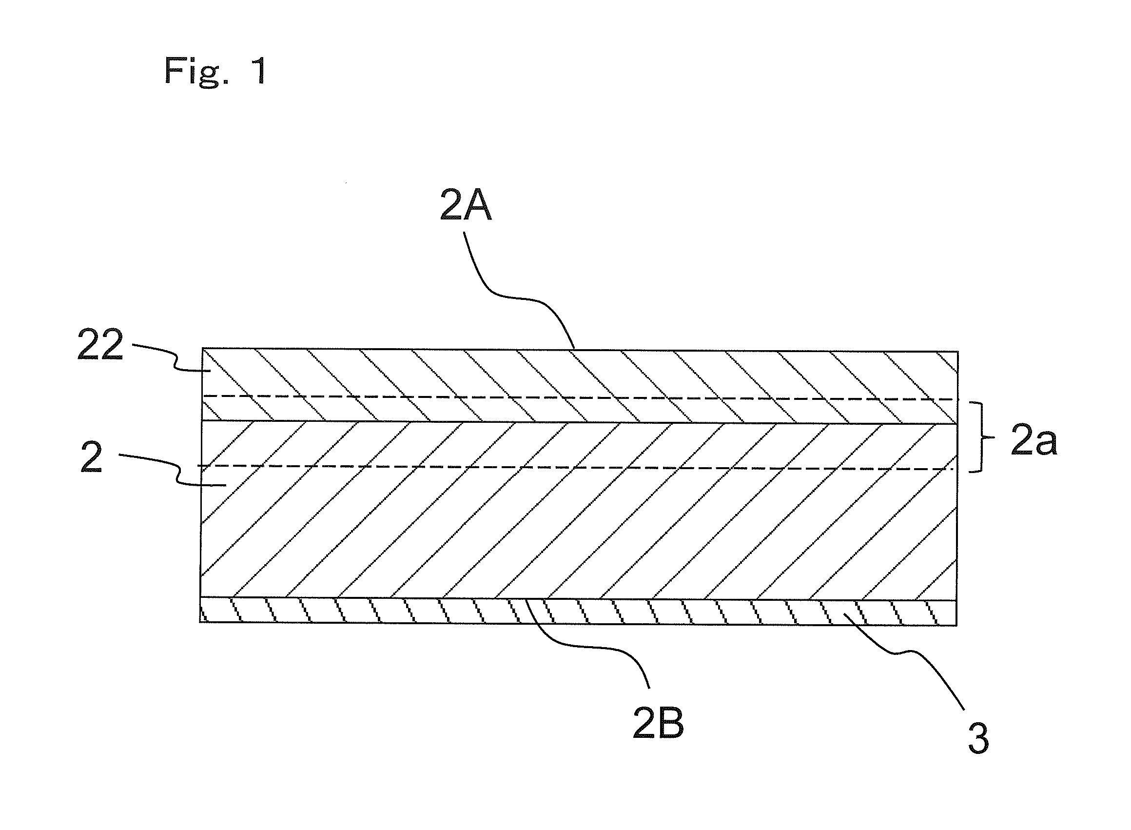
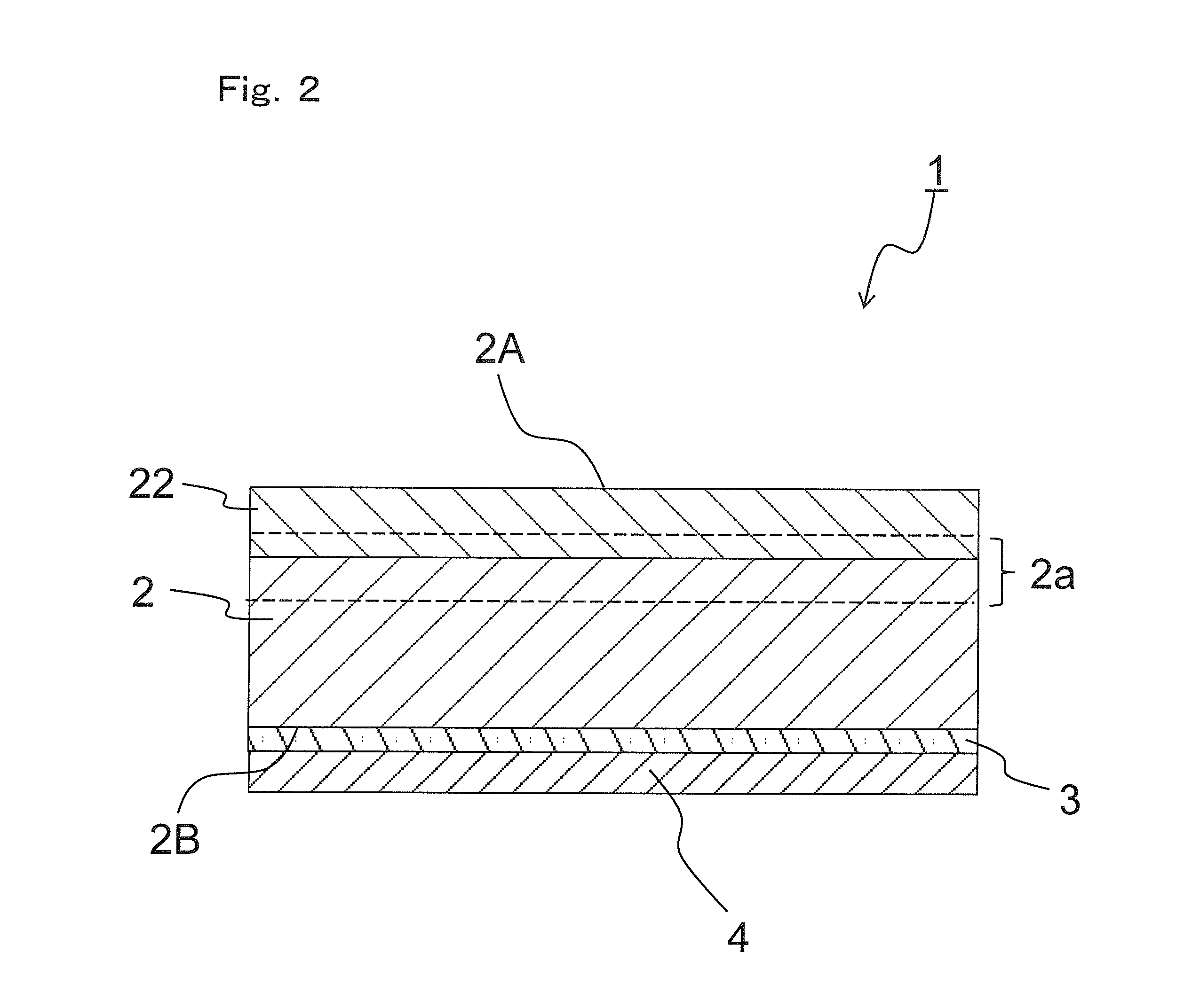
[0088]First, a p-type silicon substrate of a square of 156 mm on a side with a thickness of about 200 μm was prepared as the substrate 2. More specifically, the substrate 2 was formed by slicing a silicon ingot so that the first surface 2A and the second surface 2B are exposed. Then, the surface of the substrate 2 was slightly etched with the 10-fold diluted aqueous solution of hydrofluoric acid to remove the mechanically damaged layer and contaminated layer at the section of the substrate 2. Subsequently, phosphorus was diffused into the substrate 2 from the first surface 2A of the substrate 2, thereby forming the opposite conductivity type layer 22.

[0089]Subsequently, the first deposition step was performed by ALD. In the first deposition step, a first protective film 3 mainly containing aluminum oxide was formed over the surfaces of the substrate 2. The first deposition step was performed on the substrate 2 in a chamber of a deposition apparatus. In the first deposition step, dep...

example 2

[0094]A photoelectric conversion element 1′ produced in the same manner as in Example 1 was subjected to SIMS analysis. For SIMS, a dynamic SIMS was used. The results are shown in FIG. 7. FIG. 7 shows the results of a SIMS analysis performed on the substrate 2′, the first protective film 3′ and the second protective film 4′ of the photoelectric conversion element 1′ in the thickness direction from the surface of the second protective film 4′. In FIG. 7, numeral 7 represents the result of analysis on the photoelectric conversion element 1 before heating, numeral 8 represents the result of analysis on the photoelectric conversion element 1′ heated at 700° C. Also, in FIG. 7, numeral 9 represents the Comparative Example, in which only the first protective film 3 was formed by ALD.

[0095]For the photoelectric conversion element used for the analysis, the first protective film 3 was formed to a thickness of 40 nm, and the second protective film 4 was formed to a thickness of 20 nm. The fi...


PUM


Abstract

The method for producing a photoelectric converter of the present invention comprises a preparation step for preparing a substrate (2) that has a photoelectric conversion layer (2a) and is formed from silicon; a first film-formation step for the formation of a first protective film (3) by deposition of aluminum oxide on a top surface (2B) of the substrate (2) using the atom deposition method or chemical vapor deposition method in an atmosphere containing hydrogen; and a second film-formation step for forming a second protective film (4) by deposition of aluminum oxide on the first protective film (3) using sputtering after the first film-formation step. Moreover, the photoelectric converter of the present invention comprises a substrate that has a photoelectric conversion layer and is formed from silicon; a first protective film that is deposited on the substrate and is formed from aluminum oxide; and a second protective film that is deposited on the first protective film and is formed from aluminum oxide, wherein the concentration of hydrogen contained in the first protective film is higher than the concentration of hydrogen contained in the second protective film.

Description

TECHNICAL FIELD[0001]The present invention relates to a method for manufacturing a photoelectric conversion element and to a photoelectric conversion element.BACKGROUND ART[0002]A photoelectric conversion element, which converts light into electricity, may be provided with a protective film on the surface of the substrate to suppress the recombination carriers, generated in the photoelectric conversion layer, at the surface of the substrate. Such a protective film is generally formed by atomic layer deposition (ALD) or chemical vapor deposition (CVD) in view of damage to the surface of the substrate (see, for example, Japanese Unexamined Patent Application Publication No. 2011-249813).SUMMARY OF INVENTION[0003]When the protective film on the substrate is subjected to heat application, however, hydrogen can be released from the protective film. If hydrogen has been released from the protective film, carriers become easy to recombine at the surface of the substrate. Consequently, the ...

Claims


Application Information

Patent Timeline
IPC IPC(8): H01L31/18H01L31/0224H01L31/0216
CPCH01L31/0216H01L31/0224H01L31/1804H01L31/02167H01L31/022425Y02E10/547Y02P70/50
Inventor MIYAZAKI, SHIROHONJO, TOMOFUMINIWA, KOJIKII, HIRONORIAONO, SHIGEONISHIOKA, YOSUKE
Owner KYOCERA CORP
Why Eureka
Try Eureka