
Optical modulator, optical transmission device, and bias adjusting method

a technology of optical transmission device and optical modulator, which is applied in the direction of optical elements, optical waveguide light guides, instruments, etc., can solve the problems of large variation of loss, increased loss in optical modulator, and larger loss in sub-modulator

Active Publication Date: 2012-01-12
MITSUBISHI ELECTRIC CORP
View PDF2 Cites 18 Cited by
  • Summary
  • Abstract
  • Description
  • Claims
  • Application Information

AI Technical Summary

Benefits of technology

[0009]It is an object of the present invention to at least partially solve the problems in the conventional technology.

Problems solved by technology

However, when an optical modulator is integrated and unified on a compound semiconductor, a loss in a sub-modulator is larger than that when a sub-modulator is formed by LN, and a variation of the loss becomes large.
Therefore, a loss in an optical modulator increases, and a variation of a loss between sub-modulators becomes larger.
However, when there is a variation between a loss in a sub-modulator for the I channel and that in a sub-modulator for the Q channel, a difference occurs between an amplitude level of an optical modulation signal in the I channel and that of an optical modulation signal in the Q channel, and the modulation waveform quality becomes low.

Method used


Image

  • Optical modulator, optical transmission device, and bias adjusting method
  • Optical modulator, optical transmission device, and bias adjusting method
  • Optical modulator, optical transmission device, and bias adjusting method

Examples


first embodiment

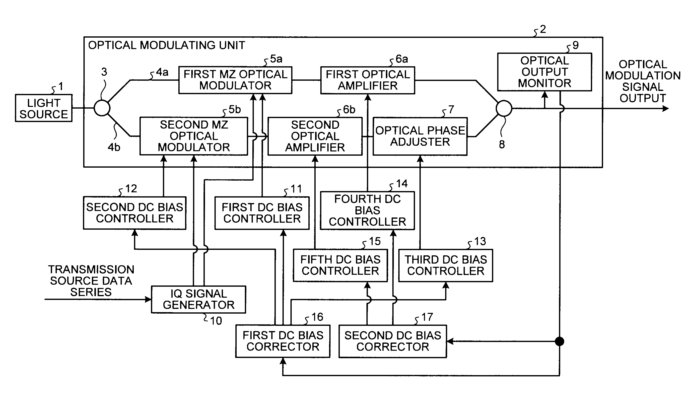
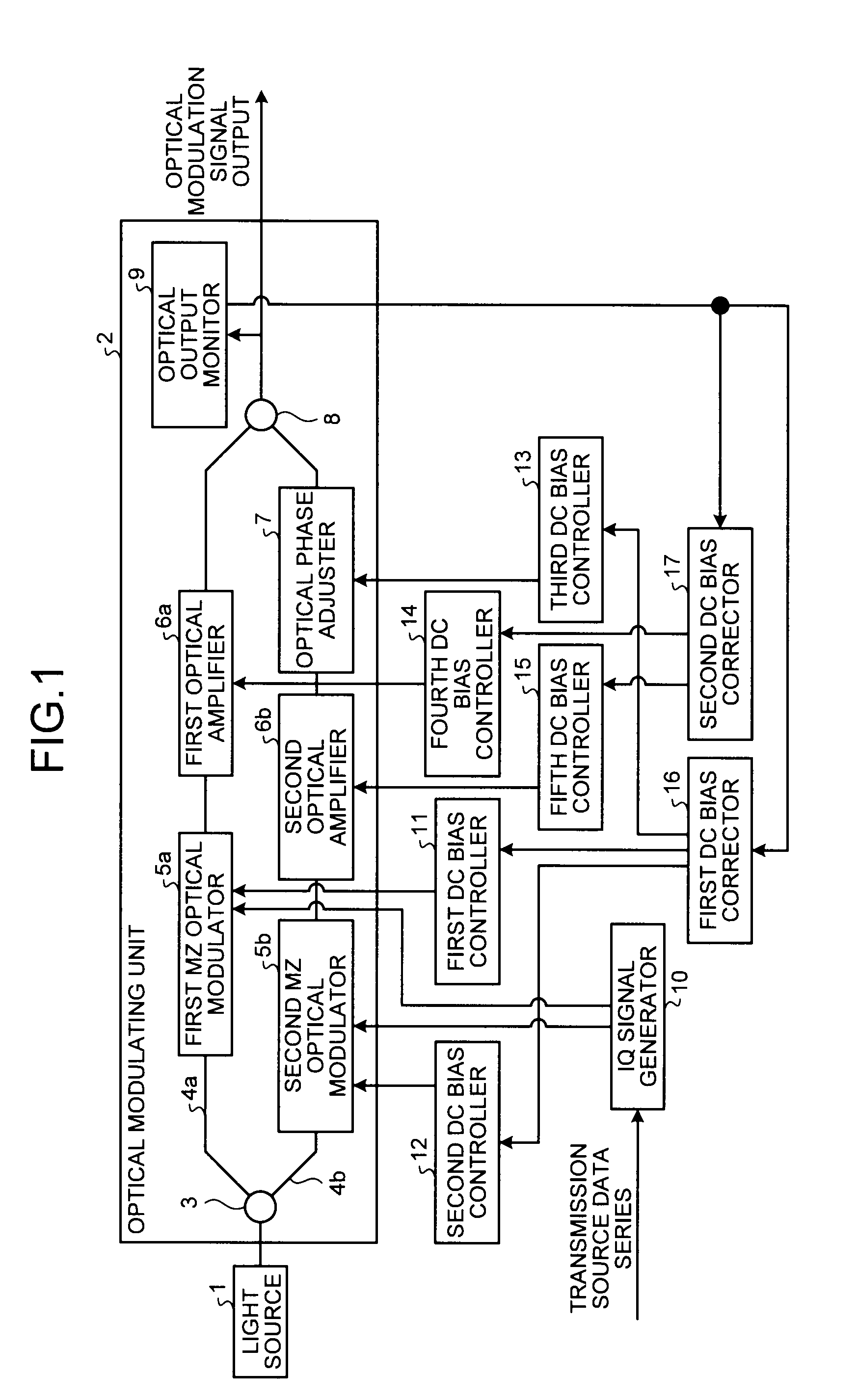
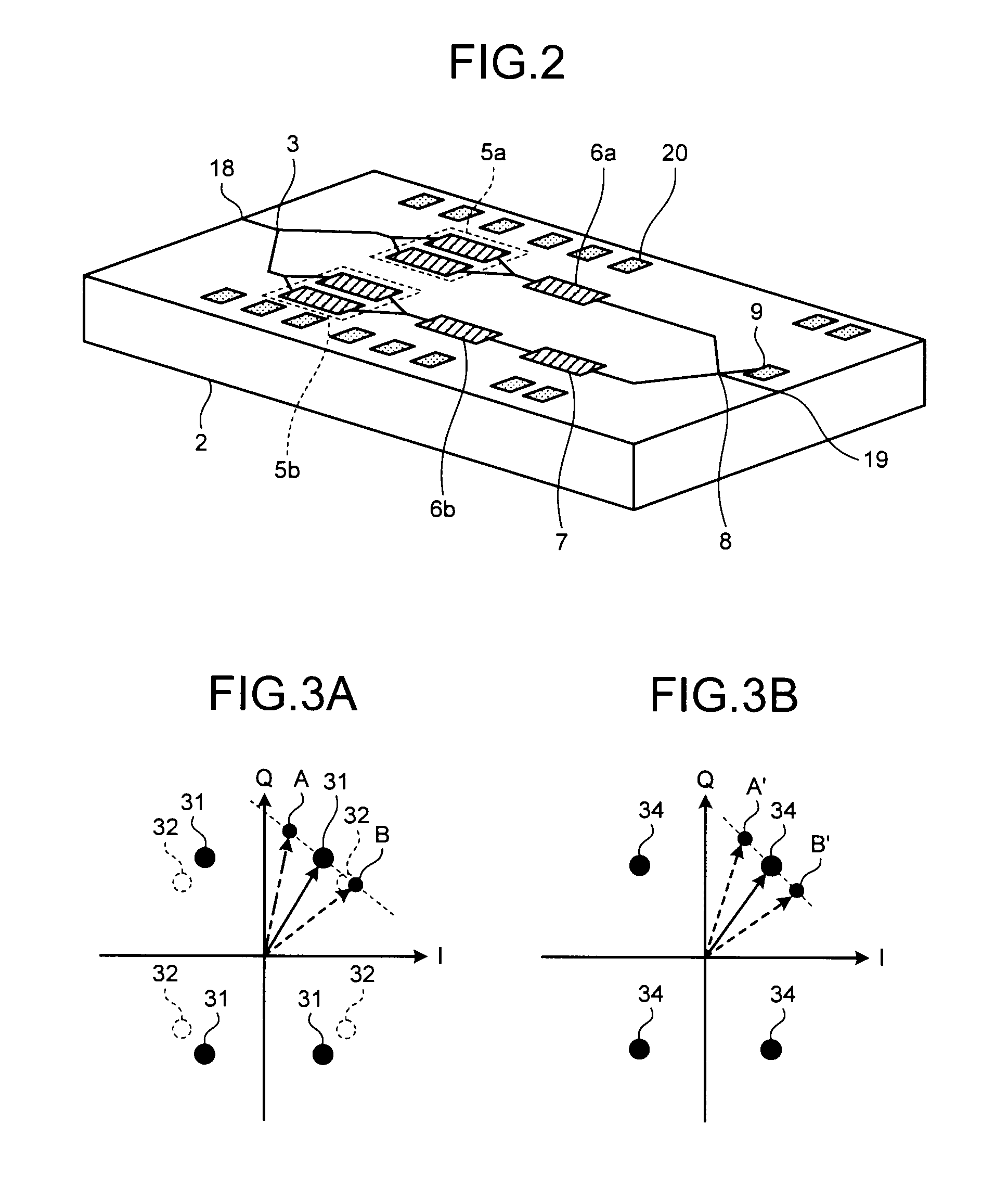
[0026]FIG. 2 is a schematic diagram of an example of the optical modulating unit 2 mounted on a substrate. In FIG. 2, constituent elements denoted by like reference numerals as those in FIG. 1 have functions identical to those in FIG. 1. The mounted optical modulating unit 2 shown in FIG. 2 includes electric terminals 20 to connect the optical modulating unit 2 with external electric signals, optical input waveguides 18 to input optical signals from outside, and an optical output waveguide 19 to output optical signals to outside, in addition to the constituent elements shown in FIG. 1. The optical input waveguides 18 are connected to the optical demultiplexing unit 3, and output light is input from the light source 1 to the optical demultiplexing unit 3. The optical output waveguide 19 is connected to the optical multiplexer 8, and outputs optical signals that are input from the optical multiplexer 8 to outside. The schematic diagram of FIG. 2 is an implementation example, actual s...

second embodiment

[0064]In the second embodiment, an amplitude of a superimposed low-frequency pulse signal is adjusted based on a characteristic (for example, a characteristic shown in FIG. 6A) of an amplification factor to a bias current input to the first optical amplifier 6a and the second optical amplifier 6b, respectively. Therefore, an adjustment error attributable to a change rate of an amplification factor of a bias signal input to the first optical amplifier 6a and a change rate of an amplification factor of a bias signal input to the second optical amplifier 6b as described above is prevented.

[0065]FIG. 6B is an example of a low-frequency pulse signal superimposed on the first optical amplifier 6a and the second optical amplifier 6b according to the second embodiment. When complementary low-frequency pulse signals are generated, the second DC bias corrector 17 generates low-frequency pulse signals such that the ratio of an amplitude “a” of a low-frequency pulse signal (a low-frequency puls...

third embodiment

[0072]In the third embodiment, two kinds of bias signals for a first optical amplifier 25a and a second optical amplifier 25b are input from the fourth DC bias controller 14 to the first optical amplifier 25a and the second optical amplifier 25b, respectively. Similarly, two kinds of bias signals for a third optical amplifier 25c and a fourth optical amplifier 25d are input from the fifth DC bias controller 15 to the third optical amplifier 25c and the fourth optical amplifier 25d, respectively. The fourth DC bias controller 14 can be configured to include a functional unit that generates a bias signal for the first optical amplifier 25a, and a functional unit that generates a bias signal for the second optical amplifier 25b. Similarly, the fifth DC bias controller 15 can be configured to include a functional unit that generates a bias signal for the third optical amplifier 25c, and a functional unit that generates a bias signal for the fourth optical amplifier 25d.

[0073]An optical...


PUM

PropertyMeasurementUnit
phaseaaaaaaaaaa
frequencyaaaaaaaaaa
strengthaaaaaaaaaa

Abstract

Included are a first modulator, a second modulator, a first optical amplifier that amplifies an output of the first modulator at an amplification factor based on a first bias signal, a second optical amplifier that amplifies an output of the second modulator at an amplification factor based on a second bias signal, an optical phase adjuster that phase-rotates an output of the second optical amplifier, an optical multiplexer that multiplexes an output of the first optical amplifier with an output of the optical phase adjuster, and a second bias corrector that generates a first pulse signal and a second pulse signal, which are complementary to each other, and obtains a first bias value and a second bias value based on a change of strength of an output signal of the optical multiplexer. The first and second pulse signals are superimposed on the first and second bias signals, respectively.

Description

BACKGROUND OF THE INVENTION[0001]1. Field of the Invention[0002]The present invention relates to an optical modulator, an optical transmission device, and a bias adjusting method.[0003]2. Description of the Related Art[0004]A conventional optical modulator that performs a Quadrature Phase Shift Keying (QPSK) modulation includes two sub-modulators (see, for example, Japanese Patent Application Laid-open No. 2008-187223 and Japanese Patent Application Laid-open No. 2008-236512). Signals of an I channel and a Q channel are input to these two sub-modulators, respectively. The two sub-modulators modulate the input signals of the I channel and the Q channel and output optical modulation signals. Among the optical modulation signals of two systems modulated by the two sub-modulators, a phase of one optical modulation signal is rotated by π / 2 (90 degrees) by using an optical phase modulator. The optical modulation signal of which a phase is rotated is combined and interfered with an optical...

Claims


Application Information

Patent Timeline
Patent Type & Authority Applications(United States)
IPC IPC(8): H04B10/04G02F1/01G02F1/035H04B10/07H04B10/516H04B10/524H04B10/556H04B10/564H04B10/61
CPCH04B10/5053H04B10/5561H04B10/50575
Inventor ARUGA, HIROSHIMOCHIZUKI, KEITASUGITATSU, ATSUSHI
Owner MITSUBISHI ELECTRIC CORP
Learn More