Supercharge Your Innovation With Domain-Expert AI Agents!

Wafer level LED package structure for increase light-emitting efficiency and method for making the same

a technology of led package structure and led package layer, which is applied in the direction of semiconductor/solid-state device manufacturing, electrical apparatus, semiconductor devices, etc., can solve the problems of easy loss of light-emitting function, increase the thickness of a reflecting insulating layer, and avoid short circuits. , the effect of increasing the light-emitting efficiency

Inactive Publication Date: 2012-01-12
HARVATEK CORPORATION
View PDF4 Cites 0 Cited by
  • Summary
  • Abstract
  • Description
  • Claims
  • Application Information

AI Technical Summary

Benefits of technology

The present invention provides a wafer level LED package structure and a method for making it that increases light-emitting efficiency. The structure includes a light-emitting unit with a reflecting insulating layer and two conductive units, and a method for making it by removing a peripheral part of the top material layer and forming an insulating layer around the outer area of the top surface of the bottom material layer. The insulating layer has two openings for exposing the positive and negative conductive layers, and the openings are filled with conductive material to form the conductive units. The structure prevents short circuits between the conductive layers and allows for normal light beam generation.

Problems solved by technology

Therefore, the LED package structure of the prior art will loss the light-emitting function easily.

Method used


Image

  • Wafer level LED package structure for increase light-emitting efficiency and method for making the same
  • Wafer level LED package structure for increase light-emitting efficiency and method for making the same
  • Wafer level LED package structure for increase light-emitting efficiency and method for making the same

Examples


Embodiment Construction

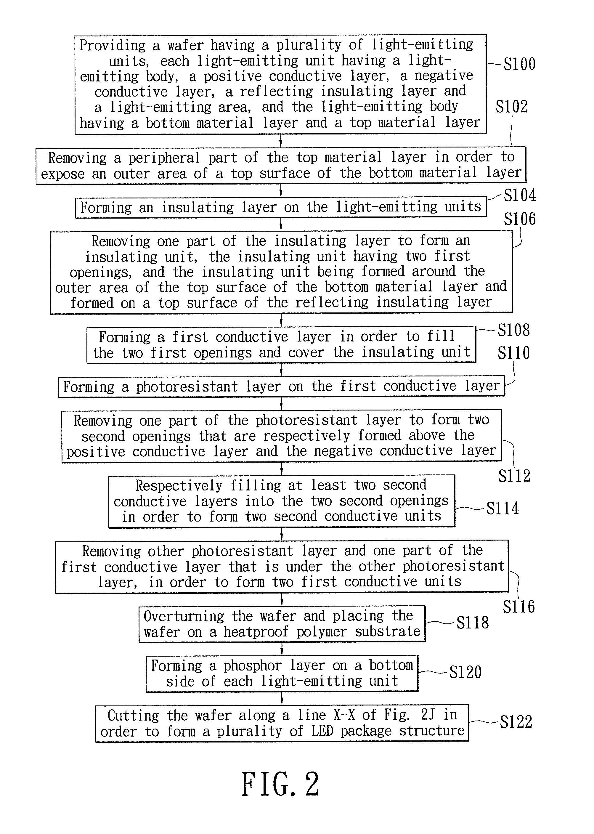
[0022]Referring to FIGS. 2 and 2A to 2K, the first embodiment of the present invention provides a method for making a wafer level LED package structure for increasing light-emitting efficiency. The method includes following steps:

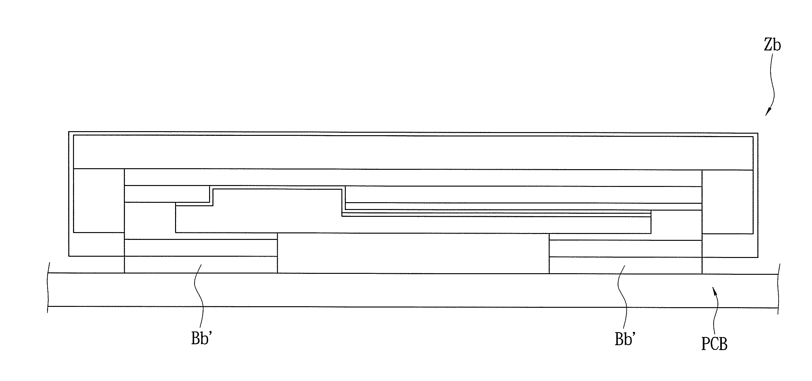
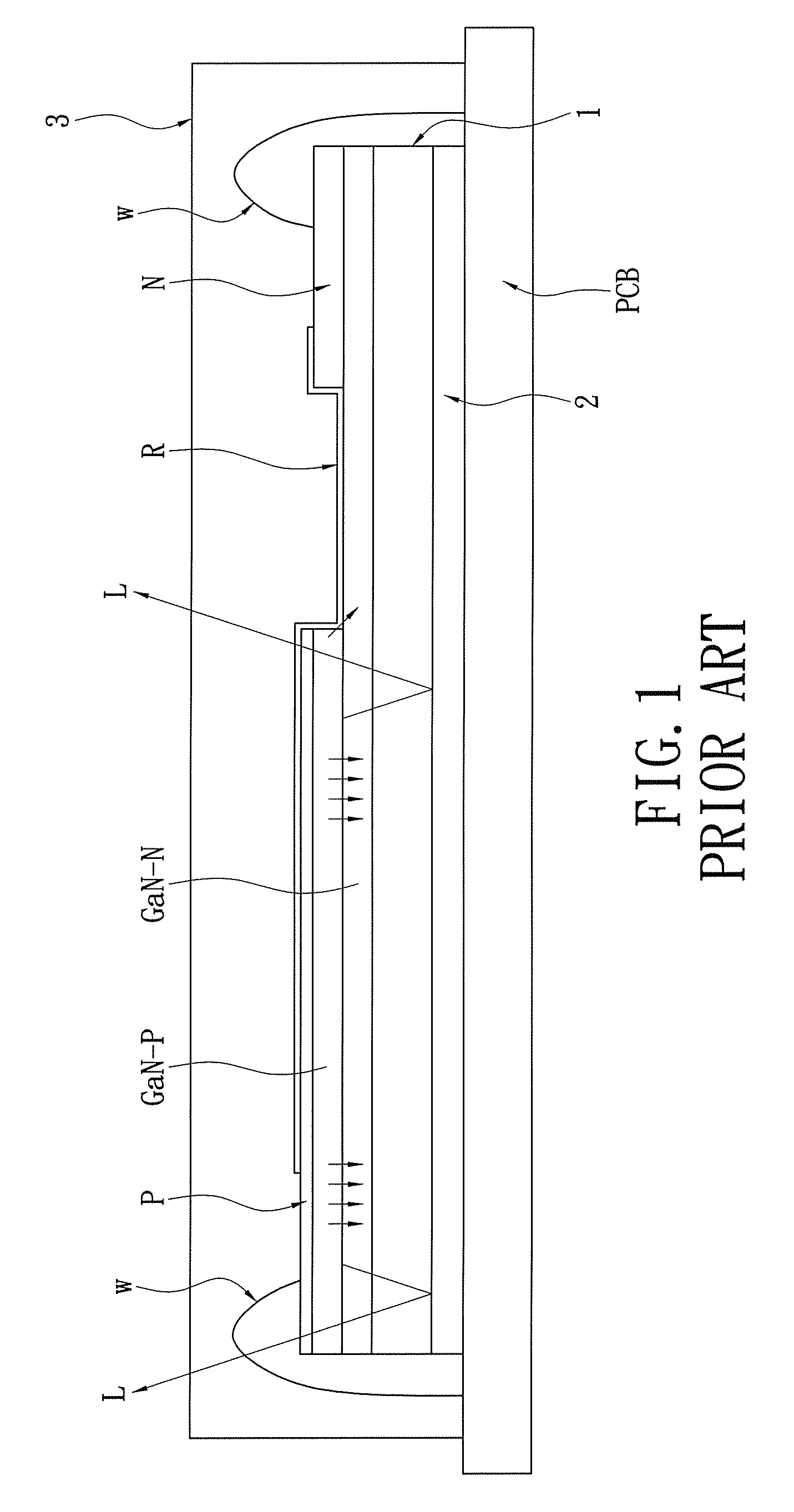
[0023]The step S100 is: referring to FIGS. 2 and 2A, providing a wafer W having a plurality of light-emitting units 1a (only shown one light-emitting units 1a in Figures), each light-emitting unit 1a having a light-emitting body 10a, a positive conductive layer Pa (P-type semiconductor material layer) and a negative conductive layer Na (N-type semiconductor material layer) formed on the light-emitting body 10a, a reflecting insulating layer 11a formed between the positive conductive layer Pa and the negative conductive layer Na and a light-emitting area Aa formed in the light-emitting body 10a, and the light-emitting body 10a having a bottom material layer Da and a top material layer Ua formed on the bottom material layer Da.

[0024]Moreover, the light-emitti...


PUM


Abstract

A wafer level LED package structure for increasing light-emitting efficiency includes: a light-emitting unit, an insulating unit, two first conductive units and two second conductive units. The light-emitting unit has a light-emitting body, a positive conductive layer, a negative conductive layer, and a reflecting insulating layer formed between the positive conductive layer and the negative conductive layer. The light-emitting body has a bottom material layer and a top material layer. The insulating unit is formed around an outer area of a top surface of the bottom material layer and formed on a top surface of the reflecting insulating layer. One first conductive unit is formed on one part of the positive conductive layer and the insulating unit, and another first conductive unit is formed on one part of the negative conductive layer and the insulating unit. The two second conductive units are respectively formed on the two first conductive units.

Description

RELATED APPLICATIONS[0001]This application is a Divisional patent application of co-pending application Ser. No. 12 / 461,742, filed on 24 Aug. 2009, now pending. The entire disclosure of the prior application Ser. No. 12 / 461,742, from which an oath or declaration is supplied, is considered a part of the disclosure of the accompanying Divisional application and is hereby incorporated by reference.BACKGROUND OF THE INVENTION[0002]1. Field of the Invention[0003]The present invention relates to a wafer level LED package structure and a method for making the same, and particularly relates to a wafer level LED package structure for increasing light-emitting efficiency and a method for making the same.[0004]2. Description of Related Art[0005]Referring to FIG. 1, the prior art provides an LED (Light Emitting Diode) package structure including: a light-emitting body 1, a positive conductive layer P and a negative conductive layer N formed on the light-emitting body 1, a dielectric layer R for...

Claims


Application Information

Patent Timeline
Patent Type & Authority Applications(United States)
IPC IPC(8): H01L33/52
CPCH01L33/38H01L33/508H01L2224/48091H01L33/62H01L2924/00014
Inventor WANG, BILYHSIAO, SUNG-YICHEN, JACK
Owner HARVATEK CORPORATION
Features
  • R&D
  • Intellectual Property
  • Life Sciences
  • Materials
  • Tech Scout
  • Unparalleled Data Quality
  • Higher Quality Content
  • 60% Fewer Hallucinations
Learn More