
Programmable soft lithography: solvent-assisted nanoscle embossing

Active Publication Date: 2012-01-19
NORTHWESTERN UNIV
View PDF20 Cites 5 Cited by
  • Summary
  • Abstract
  • Description
  • Claims
  • Application Information

AI Technical Summary

Benefits of technology

[0006]SANE combines the strengths of serial fabrication techniques (prototyping patterns, high resolution) with those of parallel ones (high throughput, large patterned areas). Thus, SANE / inSANE enables unprecedented opportunities to manipulate electronic, photonic, and magnetic properties of nanomaterials by providing a low-cost, scalable route to large-area, nanoscale patterns.

Problems solved by technology

Although rigid molds can imprint soft and semi-hard materials, they are expensive to create and brittle at nanoscale dimensions (Chou, S. Y. et al., Science 1996, 272, 85-87; Chou, S. Y. et al., Nature 2002, 417, 835-837).

Method used


Image

  • Programmable soft lithography: solvent-assisted nanoscle embossing
  • Programmable soft lithography: solvent-assisted nanoscle embossing
  • Programmable soft lithography: solvent-assisted nanoscle embossing

Examples


Embodiment Construction

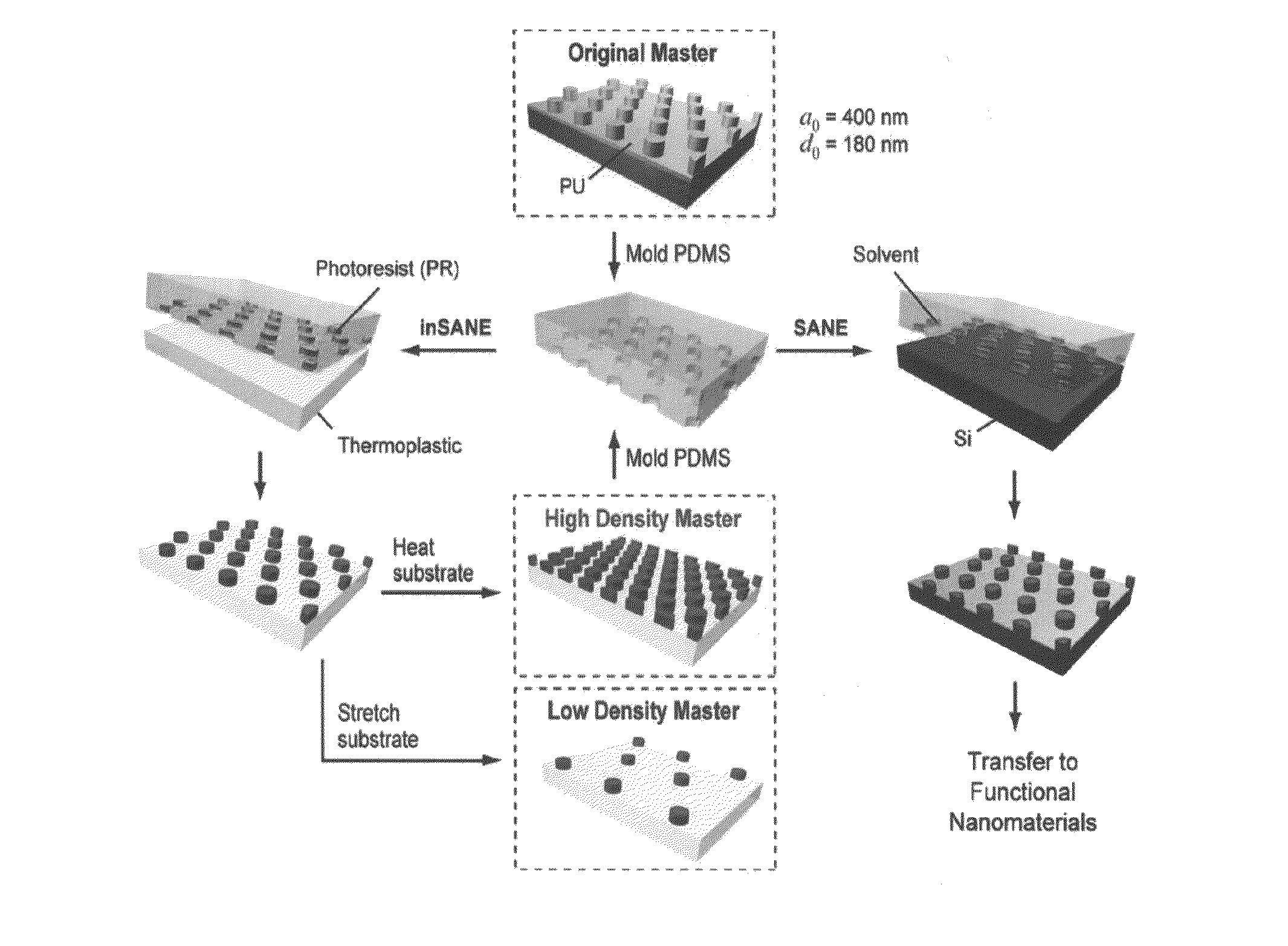
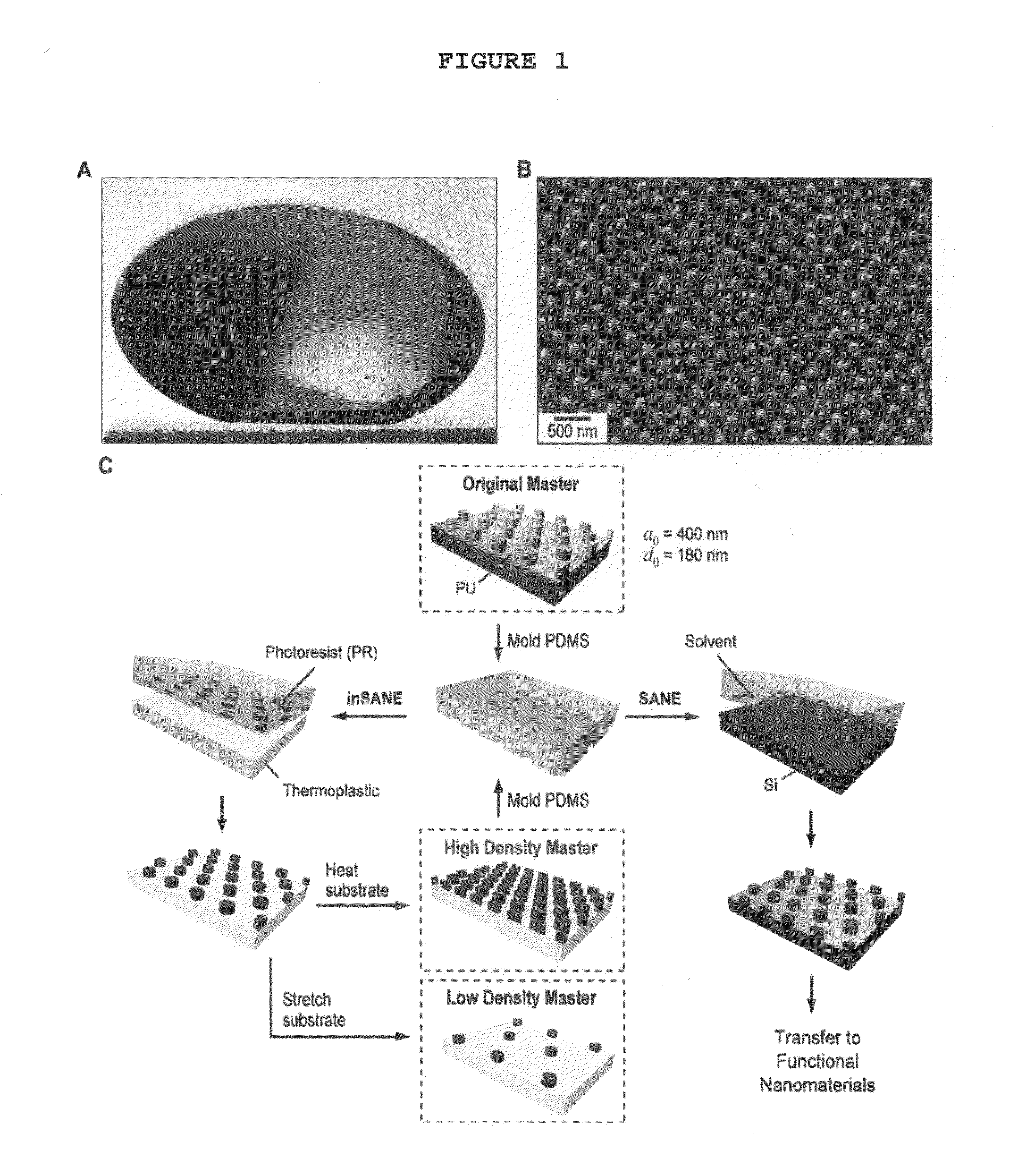
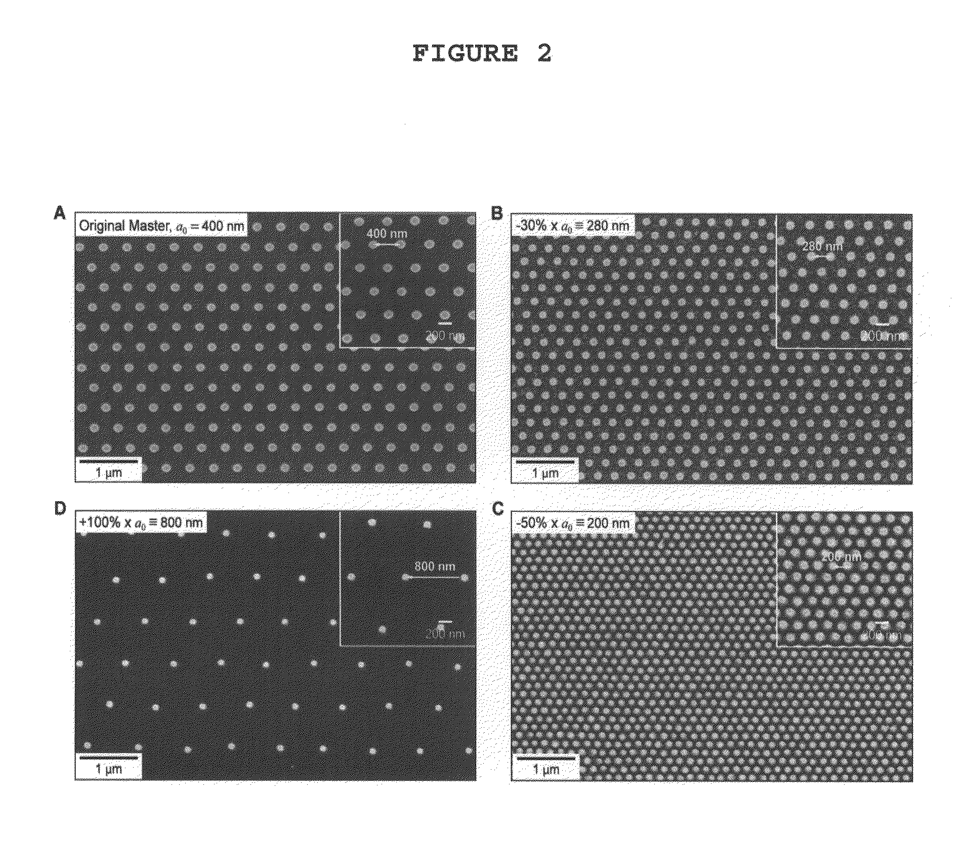
[0015]FIG. 1 illustrates certain non-limiting aspects and embodiments of the invention. Specifically, FIG. 1 summarizes how SANE is an all-polymer, parallel nanofabrication technique that can create arrays of many different patterns. Preferably, the SANE technique can generate at least four classes of different patterns from a single master: (i) arrays with higher densities; (ii) arrays with lower densities; (iii) arrays with the same densities but with smaller critical feature sizes; and (iv) arrays with different lattice symmetries. As referred to herein, “nanopattern” or “nanoscale pattern” refers to a nanometer scale structure wherein at least one lateral dimension is between the size of an individual atom and approximately 100 nm.

[0016]SANE can thus generate a wide-range of new masters and patterns that are easily transferred into functional materials and devices by conventional fabrication methods. To demonstrate these inclusive capabilities of SANE, a large-area (6-in diamete...


PUM

PropertyMeasurementUnit
Fractionaaaaaaaaaa
Fractionaaaaaaaaaa
Fractionaaaaaaaaaa

Abstract

A method of forming a nanoscale pattern on a substrate is provided, wherein the method increases or decreases the spacing of patterns on the substrate relative to a master, while keeping the pattern feature size constant. The method can alternatively reduce the pattern feature size of the substrate relative to a master, while keeping the spacing patterns constant.

Description

[0001]This application claims priority benefit from provisional application Ser. No. 61 / 365,052 filed on Jul. 16, 2010, the entirety of which is incorporated herein by reference.[0002]This invention was made with government support under grant number CMMI-0826219 and grant number EEC-0647560 awarded by the National Science Foundation. The government has certain rights in the invention.FIELD OF THE INVENTION[0003]The present invention relates generally to an all-moldable nanofabrication method that can generate, from a single master, large-area nanoscale patterns with programmable densities, fill factors, and lattice symmetries.BACKGROUND OF THE INVENTION[0004]Molding as a means to replicate functional and artisanal masters can be traced from the manufacturing of Mesopotamian tools to the casting of Renaissance statues. Recently, molding at the nanoscale has driven the production of high-density optical and magnetic storage media (Kang, S. et al., Opt. Eng. 2000, 39, 689-694; Wu, W. ...

Claims


Application Information

Patent Timeline
IPC IPC(8): B29C33/40
CPCB29C33/3857B29C33/405B29C33/424B29C33/40B29C61/02B29C33/3878B29C55/005
Inventor ODOM, TERI W.LEE, MIN HYUNGHUNTINGTON, MARK D.ZHOU, WEI
Owner NORTHWESTERN UNIV
Learn More