
Semiconductor device that performs refresh operation

a technology of a semiconductor device and a refresh operation, applied in the field of semiconductor devices, can solve the problems of information loss and less flexibility in the control performed by the controller

Inactive Publication Date: 2012-01-19
LONGITUDE LICENSING LTD
View PDF4 Cites 84 Cited by
  • Summary
  • Abstract
  • Description
  • Claims
  • Application Information

AI Technical Summary

Problems solved by technology

In the DRAMs, because a plurality of pieces of information are stored as electric charges in capacitors that are included in a plurality of memory cells, information is lost due to a leak current if a refresh operation is not performed periodically.
However, the semiconductor devices disclosed in the above conventional techniques have an event such that, because the number of times of the refresh command to be issued within a period of 64 msec is fixed, there is less flexibility in terms of control performed by a controller.

Method used


Image

  • Semiconductor device that performs refresh operation
  • Semiconductor device that performs refresh operation
  • Semiconductor device that performs refresh operation

Examples


first embodiment

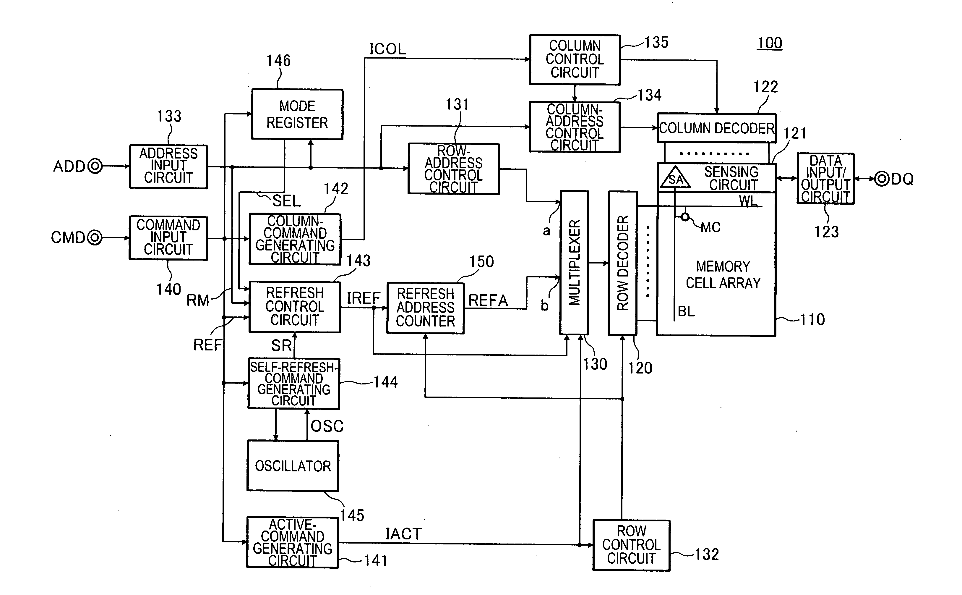
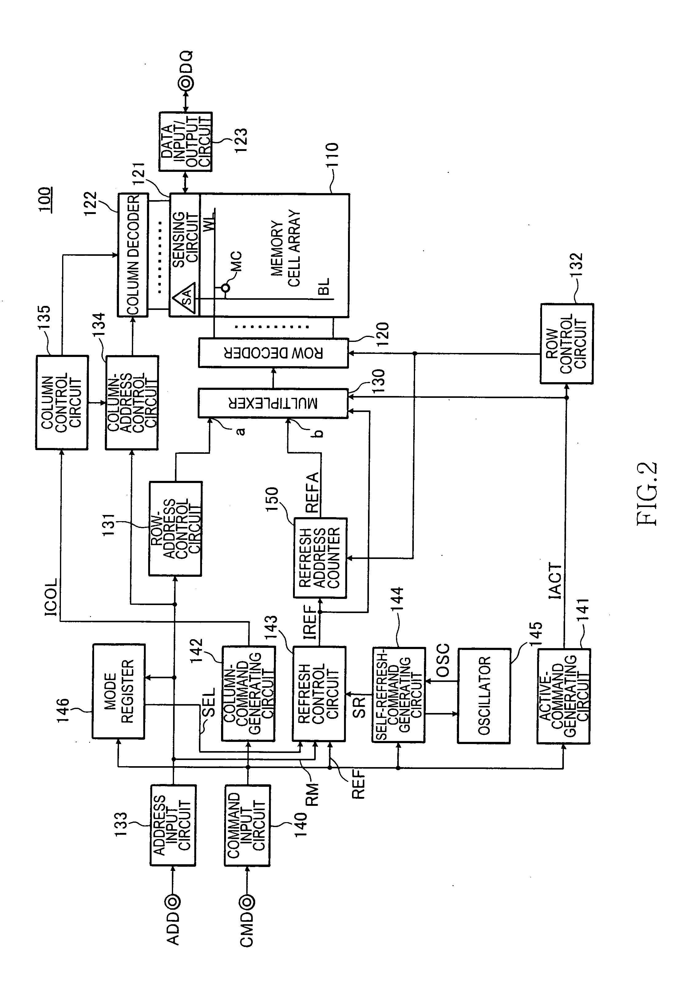
[0031]FIG. 2 is a block diagram showing a configuration of a semiconductor device 100 according to the present invention.

[0032]As shown in FIG. 2, the semiconductor device 100 according to the first embodiment includes a memory cell array 110 constituted by a plurality of memory cells MC. A plurality of word lines WL and a plurality of bit lines BL intersect each other in the memory cell array 110 and the memory cells MC are arranged at the intersections of the word lines WL and the bit lines BL. Note that FIG. 2 only shows one memory cell MC that is arranged at an intersection of one word line WL and one bit line BL.

[0033]The selection of the word lines WL is performed by a row decoder 120. Further, the bit lines BL are connected to corresponding sense amplifiers SA in a sensing circuit 121, and the sense amplifier SA selected by a column decoder 122 is connected to a data input / output circuit 123 that is connected to a data input / output terminal DQ. During a read operation, read d...

second embodiment

[0068]the present invention is explained next.

[0069]FIG. 10 is a block diagram showing a configuration of a semiconductor device 100a according to the second embodiment.

[0070]As shown in FIG. 10, the semiconductor device 100a according to the second embodiment differs from the semiconductor device 100 shown in FIG. 2 in that it includes a temperature detecting circuit 200, and a temperature detection signal T as an output of the temperature detecting circuit 200 is supplied to the refresh control circuit 143. Since other configurations of the semiconductor device 100a are identical to those of the semiconductor device 100 shown in FIG. 2, like constituent elements are denoted by like reference characters and redundant explanations thereof will be omitted.

[0071]The temperature detecting circuit 200 is a circuit that measures a chip temperature (for example, a temperature of a substrate on which the memory cell array 110 is formed), compares the measured chip temperature with a predet...


PUM


Abstract

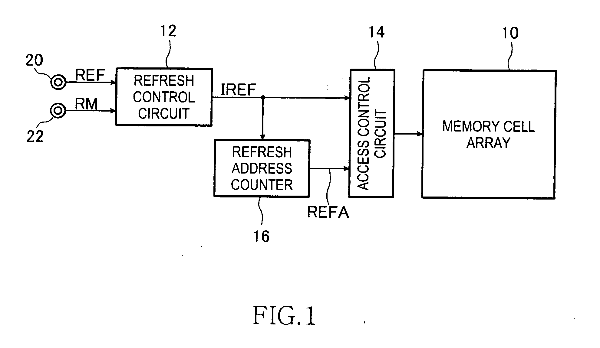
To include a refresh control circuit that generates a refresh execution signal in response to a refresh command supplied from outside, and a refresh address counter that performs a counting operation in response to activation of the refresh execution signal. The refresh control circuit generates the refresh execution signal 2n times in response to one supply of the refresh command, where n is an integer equal to or larger than 0 and equal to or less than k. The value of n is variable based on a refresh-mode specifying signal supplied from outside in synchronization with the refresh command. With this configuration, for example, a frequency of generation of the refresh execution signal in response to one supply of the refresh command can be changed dynamically, flexible control can be performed by a controller.

Description

BACKGROUND OF THE INVENTION[0001]1. Field of the Invention[0002]The present invention relates to a semiconductor device, and more particularly relates to a semiconductor device that performs a refresh operation in response to a refresh command issued from outside.[0003]2. Description of Related Art[0004]DRAMs (Dynamic Random Access Memories) that are typical semiconductor devices are volatile semiconductor memory devices. In the DRAMs, because a plurality of pieces of information are stored as electric charges in capacitors that are included in a plurality of memory cells, information is lost due to a leak current if a refresh operation is not performed periodically. Therefore, it is necessary to refresh all memory cells before the information is lost due to the leakage current. A period(=tREF) of 64 milliseconds (msec) is defined as a standard for refreshing all the memory cells. Accordingly, refresh commands issued by a controller are issued in such a manner that all word lines as...

Claims


Application Information

Patent Timeline
IPC IPC(8): G11C11/402
CPCG11C11/406G11C11/404G11C11/40611
Inventor NARUI, SEIJI
Owner LONGITUDE LICENSING LTD
Learn More