

Array architecture for reduced voltage, low power, single poly EEPROM
- Summary
- Abstract
- Description
- Claims
- Application Information
AI Technical Summary
Benefits of technology
Problems solved by technology
Method used
Image

Examples
Embodiment Construction
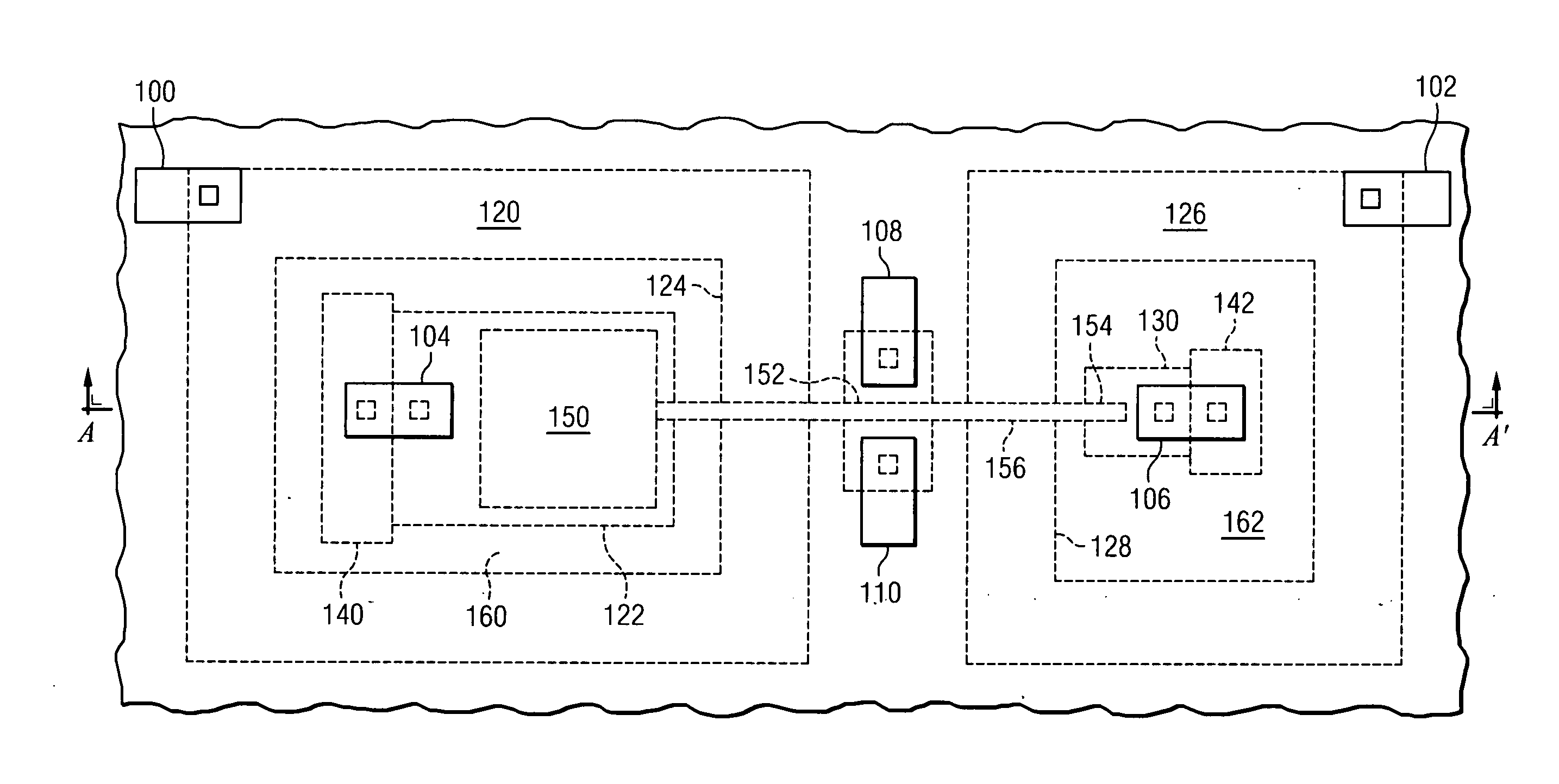
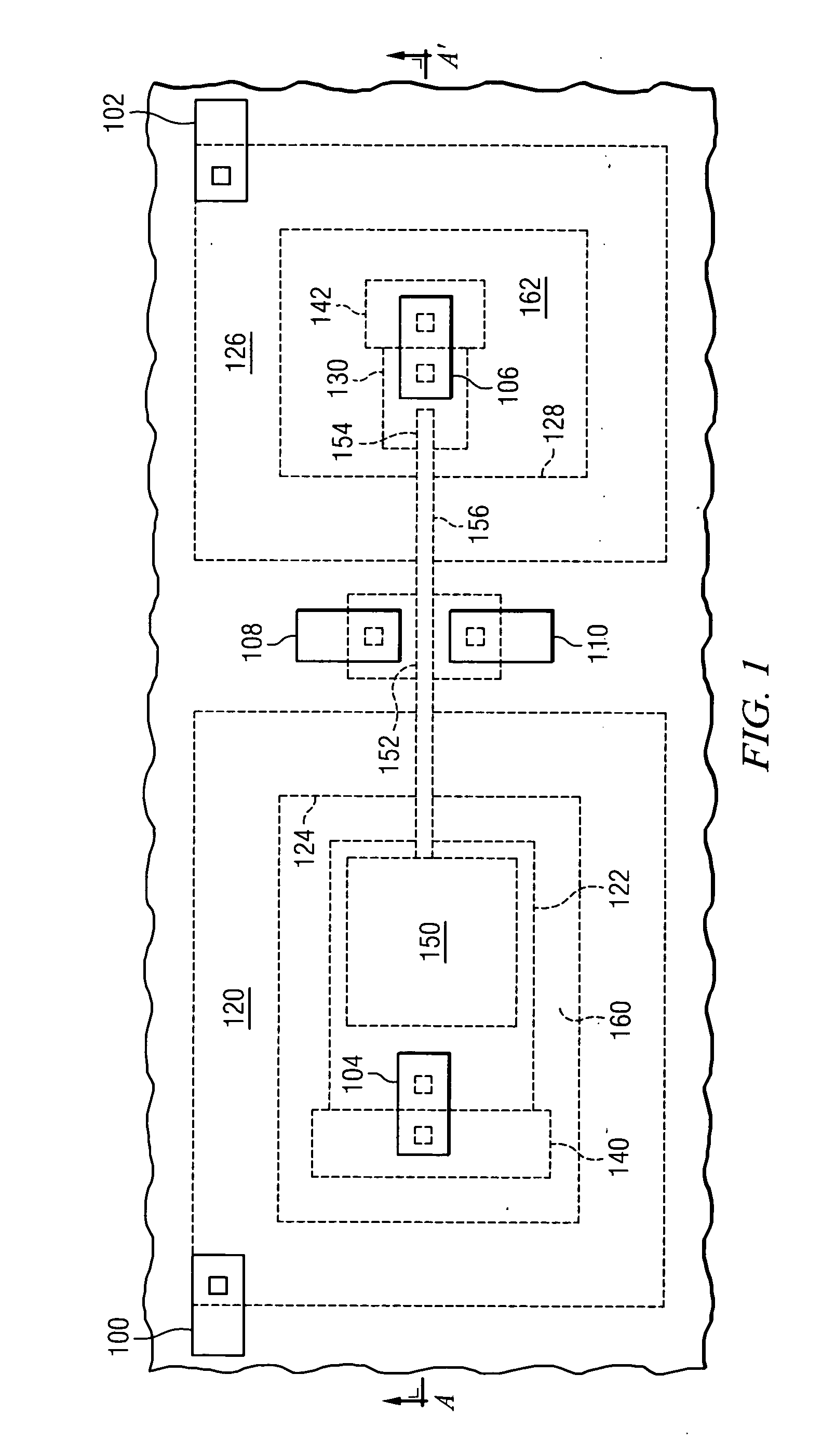
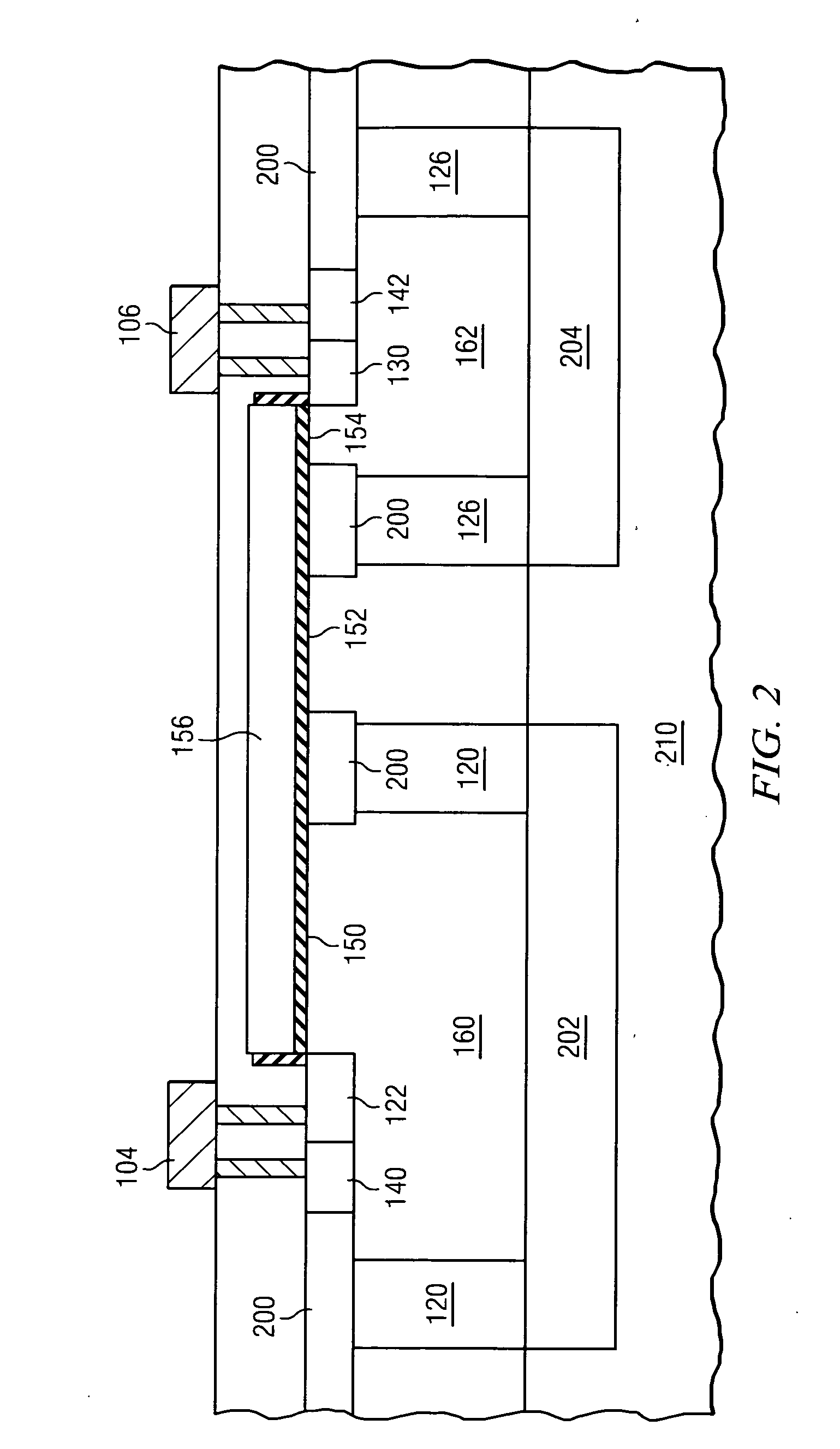
[0019]Preferred embodiments of the present invention provide significant advantages over previous memory array architectures using single polycrystalline silicon EEPROM memory cells as will become evident from the following detailed description. The present inventors have disclosed a single polycrystalline silicon EEPROM cell in U.S. patent application Ser. No. 12 / 462,076, (TI-66531), filed Jul. 28, 2009, and incorporated herein by reference in its entirety. The following discussion briefly describes that EEPROM memory cell to provide a more complete understanding of the present invention. In the following discussion, P and N are used to indicate semiconductor conductivity type. A “+” or “−” sign after the conductivity type indicates a relatively high or low doping concentration, respectively, of the semiconductor region. Furthermore, the same reference numerals are used in the drawing figures to indicate common circuit elements.
[0020]Referring to FIG. 1, there is a top view of a si...
PUM
 Abstract
Description
Claims
Application Information