

Semiconductor growing apparatus
a growing apparatus and semiconductor technology, applied in the direction of chemically reactive gases, coatings, crystal growth processes, etc., can solve the problems of difficult formation of ring-shaped hollows in susceptors formed with castings, high susceptor cost, uneven etc., to achieve the effect of improving the temperature distribution of substrates
- Summary
- Abstract
- Description
- Claims
- Application Information
AI Technical Summary
Benefits of technology
Problems solved by technology
Method used
Image

Examples
first embodiment
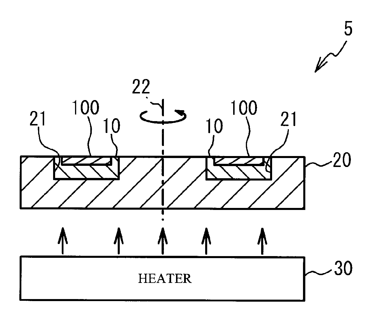
[0022]A description will be given of a semiconductor growing apparatus 5 in accordance with a first embodiment. The semiconductor growing apparatus 5 is used in a deposition process for forming a semiconductor layer on a substrate 100. In concrete, the semiconductor growing apparatus 5 is used in a deposition process in which the substrate 100 is heated. The deposition process is, for example, a vapor-phase deposition such as CVD (Chemical Vapor Deposition), MOCVD (Metal Organic Chemical Vapor Deposition) or Plasma CVD (Plasma Chemical Vapor Deposition).
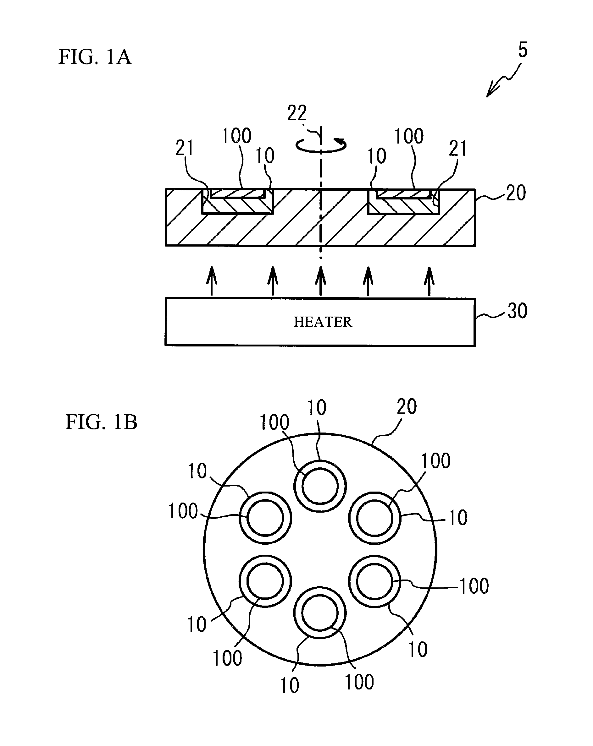
[0023]FIG. 1A illustrates a schematic cross sectional view of the semiconductor growing apparatus 5 in accordance with the first embodiment. FIG. 1B illustrates a schematic top view of the semiconductor growing apparatus 5 of FIG. 1A. The semiconductor growing apparatus 5 has a susceptor 10, a tray 20, and a heater 30. The susceptor 10 and the tray 20 are provided in a chamber in a deposition process.
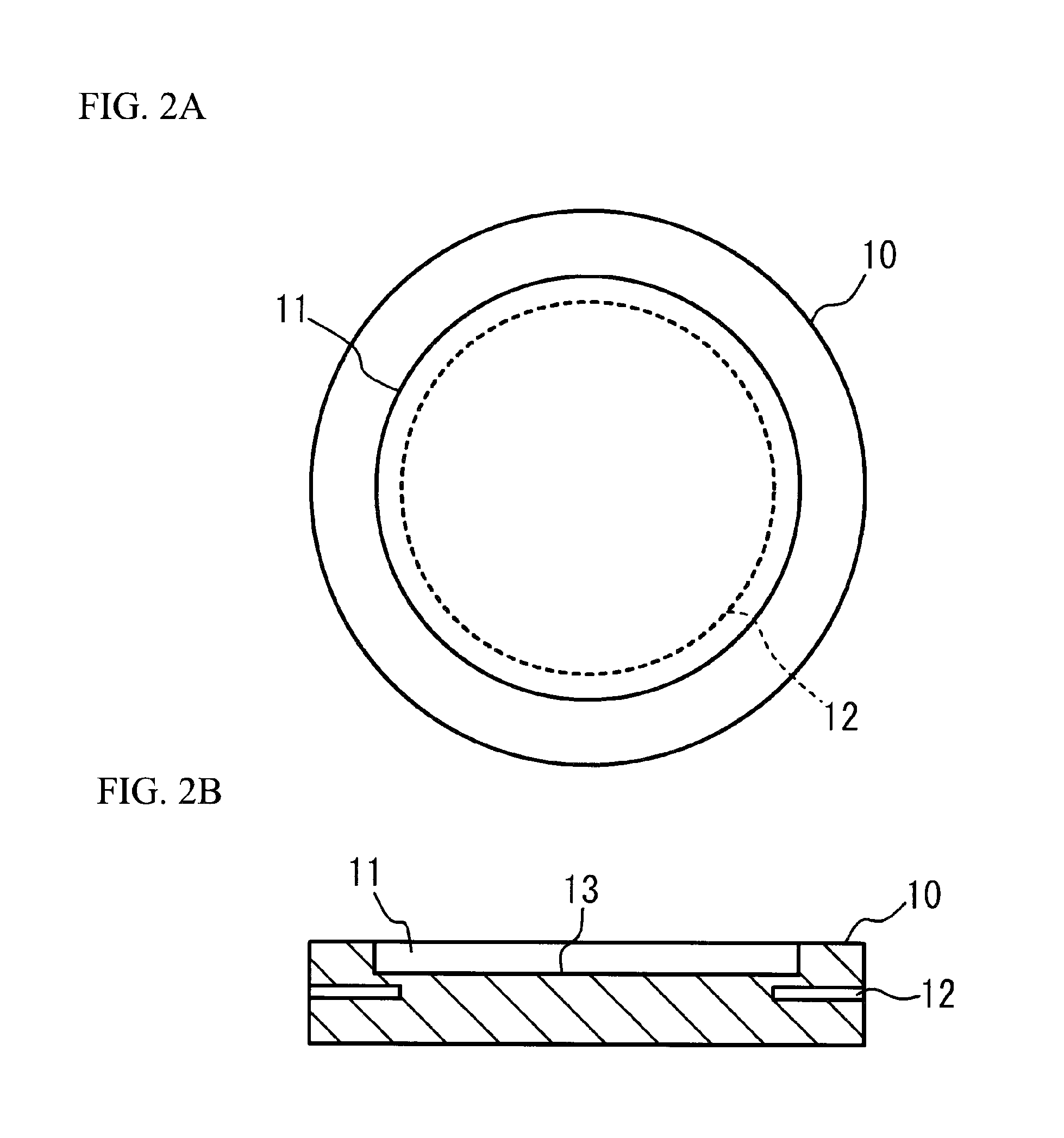
[0024]The susceptor 10 holds the ...
second embodiment
[0043]FIG. 5A through FIG. 5C illustrate a cross sectional view of the susceptor 10 of the semiconductor growing apparatus 5 in accordance with a second embodiment. The shape of the groove 12 or the number of the groove 12 of the susceptor 10 of the semiconductor growing apparatus 5 is modified in order to adjust the temperature distribution more particularly. The other structure is the same as the first embodiment.
[0044]For example, the cross sectional area of the groove 12 gets smaller, in accordance with the groove 12 leaves from the circumference of the susceptor 10. In FIG. 5B, the susceptor 10 has a plurality of the grooves 12 having a different depth from the side face of the susceptor 10. In FIG. 5B, the depth of one groove 12 on the side of the mounting face 13 is longer than that of another groove 12 on the side of the lower face of the susceptor 10. In FIG. 5C, the groove 12 is inclined with respect to the mounting face 13. In FIG. 5C, the groove 12 is inclined so that a ...
third embodiment
[0047]FIG. 6 schematically illustrates a top view of the tray 20 and the susceptor 10 of the semiconductor growing apparatus 5 in accordance with a third embodiment. The susceptor 10 of the semiconductor growing apparatus 5 in accordance with the third embodiment is different from that of the first embodiment, in a point that the groove 12 is not formed throughout the side face of the susceptor 10. The other structure is the same as the first embodiment.
[0048]For example, the temperature of a part of the circumference portion of the mounting face 13 of the susceptor 10 may be high in the deposition process because of a relative positional relationship between the heater 30 and the tray 20, the shape of the tray 20 or the like. In this case, the groove 12 may not be formed throughout the side face of the susceptor 10. The groove 12 may be formed at a position corresponding to the portion of the mounting face 13 in which temperature tends to be higher.
[0049]For example, in FIG. 6, it ...
PUM
| Property | Measurement | Unit |
|---|---|---|
| semiconductor | aaaaa | aaaaa |
| area | aaaaa | aaaaa |
| depth | aaaaa | aaaaa |
Abstract
Description
Claims
Application Information