
Patsnap Eureka
For R&D, Patsnap Eureka makes reading and utilizing patents & technical documents easy.
Patsnap Eureka AIR
Designed for self-driven R&D workflows. Generate viable solutions, solve complex R&D challenges, empower your innovation with AI.

Patsnap Eureka Materials
Designed for material experts only. Revolutionize your material R&D, from search, analyze, to developing new materials.

TechResearch
Generate reliable direction feasibility study reports for your R&D in just a few steps.

TechSeek
Discover and master advanced knowledge NOW. Basics, ideas, possibilities, all at once.

TechMind
As an expert in R&D Theories, TechMind can generates customized viable solutions instantly.

TechRisk
Analyze your overall solution with one click, know your potential R&D risks in advance.

TechMonitor
Get weekly tech updates, stay abreast of the latest tech innovations and key insights.
Semiconductor storage device
- Summary
- Abstract
- Description
- Claims
- Application Information
AI Technical Summary
Problems solved by technology
Method used
Image

Examples
first embodiment
[First Embodiment]
[0032][Configuration]
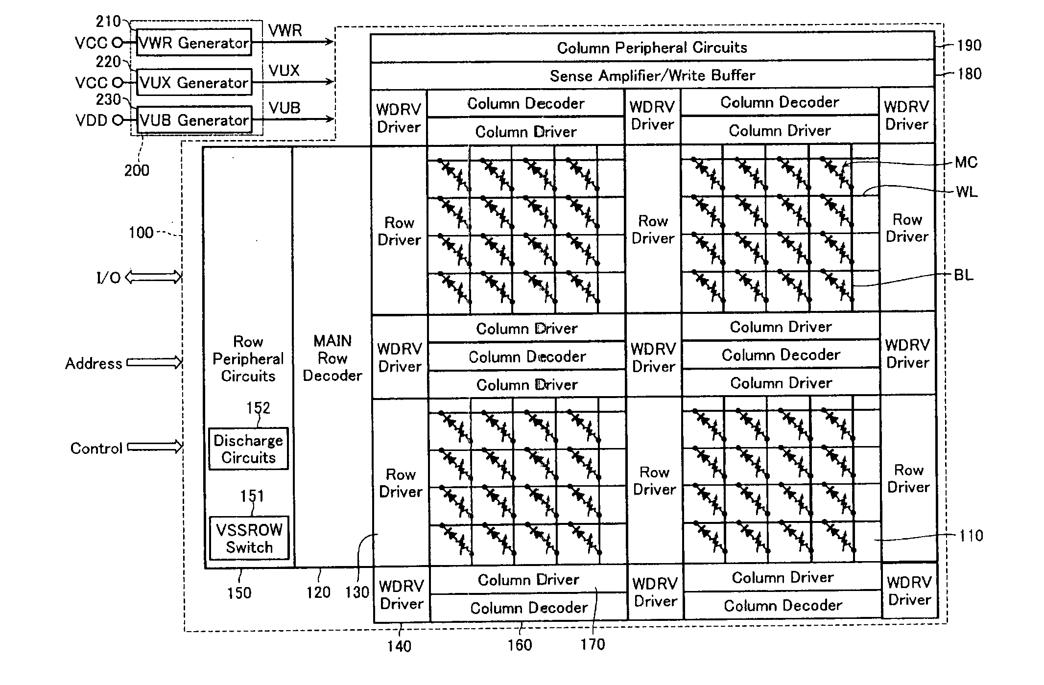
[0033]FIG. 1 is a block diagram of a semiconductor storage device (a non-volatile memory) according to a first embodiment. The semiconductor storage device according to the embodiment includes a memory cell array core portion 100 surrounded by a dotted line in FIG. 1 and power circuits 200 configured to generate and supply a voltage to be used for the memory cell array core portion 100.
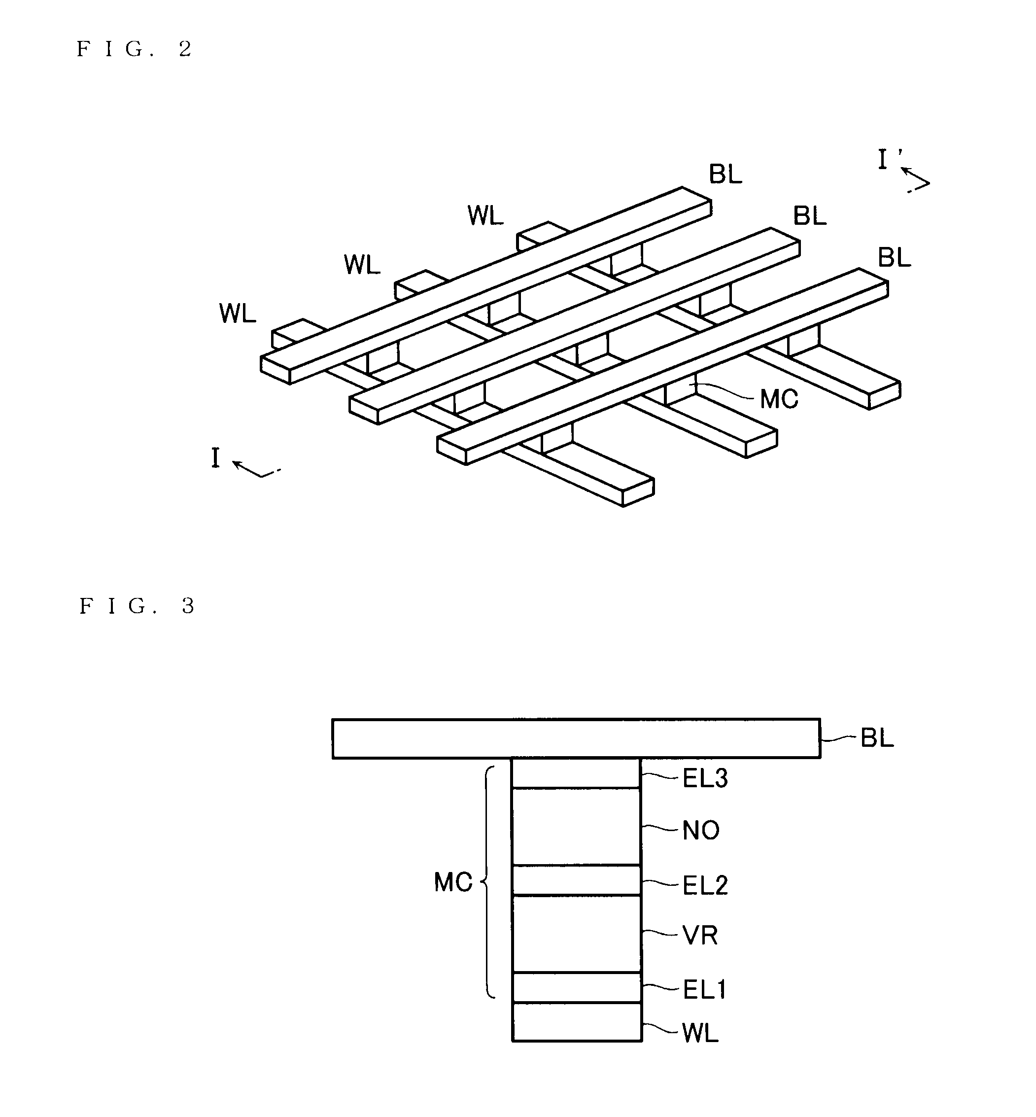
[0034]The memory cell array core portion 100 includes memory cell arrays 110, row control circuits, and column control circuits. Each of the memory cell arrays 110 includes multiple word lines WL extending in a row direction, multiple bit lines BL extending in a column direction which crosses the word lines WL, multiple memory cells MC provided at intersections between word lines WL and bit lines BL. The word lines WL are divided into multiple groups each including a predetermined number of word lines WL based on main word lines. Likewise, the bit lines BL are di...
second embodiment
[Second Embodiment]
[0102][Configuration]
[0103]Next, a description is given of a semiconductor storage device according to a second embodiment. FIG. 21 is a circuit diagram of discharge circuits 152 according to the second embodiment. Note that in the second embodiment, the same components as those in the first embodiment are denoted by the same reference numerals, and a description thereof will be omitted.
[0104]A difference between the second embodiment and the first embodiment is a configuration of a voltage generator 30. In this embodiment, the voltage generator 30 outputs a voltage VREF_SLOPE which is lowered stepwise.
[0105]The voltage generator 30 includes a PMOS transistor 31, multiple resistors 32(l) to 32(n) and 33(l) to 33(n) which form a split resistor, multiple switches 34 (l) to 34 (n+1), 35(l) to 35(n), 36, and 37, and an operational amplifier (differential amplifier) 38.
[0106]A voltage VSETH is applied to a source of the PMOS transistor 31. A drain thereof is connected ...
PUM
 Abstract
Description
Claims
Application Information
 - R&D Engineer
- R&D Manager
- IP Professional
- Industry Leading Data Capabilities
- Powerful AI technology
- Patent DNA Extraction
Browse by: Latest US Patents, China's latest patents, Technical Efficacy Thesaurus, Application Domain, Technology Topic, Popular Technical Reports.
© 2024 PatSnap. All rights reserved.Legal|Privacy policy|Modern Slavery Act Transparency Statement|Sitemap|About US| Contact US: help@patsnap.com