Semiconductor Through-Wafer Electrical Signal-Carrying Waveguide

Inactive Publication Date: 2012-02-02
IBM CORP
View PDF6 Cites 8 Cited by
  • Summary
  • Abstract
  • Description
  • Claims
  • Application Information

AI Technical Summary

Benefits of technology

[0005]A through-wafer electrical signal communication apparatus and method utilize a semiconductor substrate having a first surface, a second surface and a continuous peripheral edge. The first surface is an active device surface supporting active integrated circuit components and the second surface is a back surface. An electromagnetic waveguide supports electrical signal communication through the semiconductor substrate between the first and second surfaces. The waveguide has an electrically conductive waveguide boundary structure surrounding a waveguide interior region formed by a portion of the semiconductor substrate. The waveguide is sized

Problems solved by technology

A disadvantage of this approach is that optical signal processing is required to modulate and demodulate the optical c

Method used


Image

  • Semiconductor Through-Wafer Electrical Signal-Carrying Waveguide
  • Semiconductor Through-Wafer Electrical Signal-Carrying Waveguide
  • Semiconductor Through-Wafer Electrical Signal-Carrying Waveguide

Examples


first example embodiment

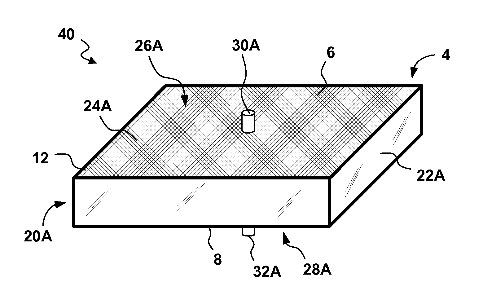
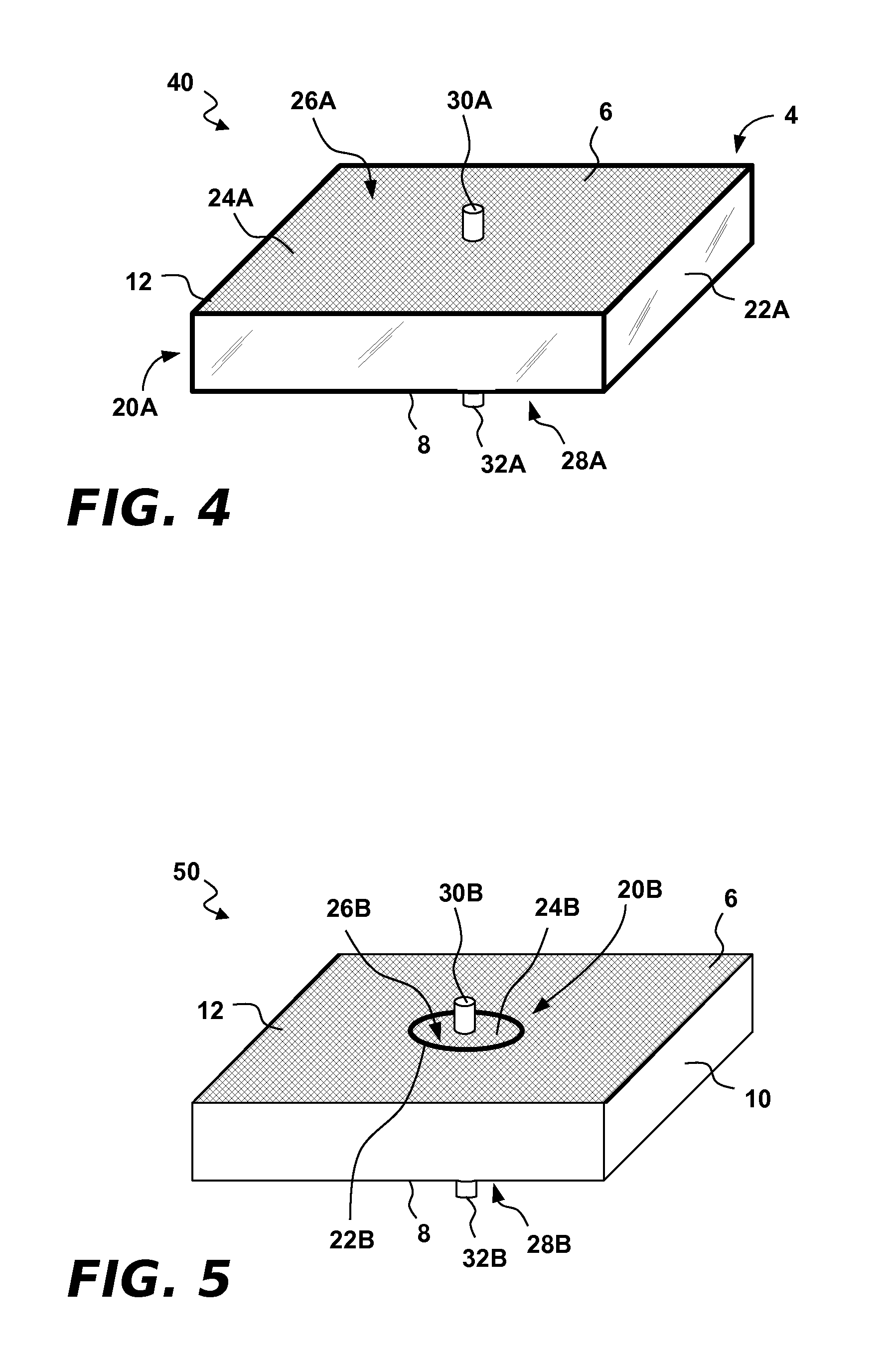
[0020]Turning now to FIG. 4, an apparatus 40 with through-wafer electrical signal communication capability is shown. The apparatus 40 is constructed from the semiconductor substrate 4 of FIG. 1 and further includes the waveguide 20 of FIG. 2 embodied as a real waveguide 20A. The real waveguide 20A includes a real waveguide boundary structure 22A formed by an electrically conductive material that surrounds the semiconductor peripheral edge 10. For example, the electrically conductive material may comprise an electrically conductive (e.g., metal) sleeve in which the semiconductor substrate 4 is situated. The conductive sleeve may either short the substrate peripheral edge 10 or an insulation layer could be added to electrically isolate the semiconductor substrate 4 from the conductive sleeve. Alternatively, the electrically conductive material may comprise an electrically conductive (e.g., metallization) coating applied to the substrate peripheral edge 10, or to an insulation layer su...

second example embodiment

[0023]Turning now to FIGS. 5-7, another apparatus 50 with through-wafer electrical signal communication capability is shown. The apparatus 50 is constructed from the semiconductor substrate 4 of FIG. 1 and further includes the waveguide 20 of FIG. 2 embodied as a virtual waveguide 20B. The virtual waveguide 20B includes a virtual waveguide boundary structure 22B surrounding a virtual waveguide interior region 24B. The virtual waveguide boundary structure 22B is formed by an electrically conductive region of the semiconductor substrate 4. This region comprises free semiconductor charge carriers that have been excited into a conduction band by incident light 52 emitted by a light source 54 (see FIG. 7). The incident light 52 changes the index of refraction within the electrically conductive region of the semiconductor substrate 4 (relative to the electromagnetic signal being propagated). This produces a dielectric waveguide whose wave containment properties are determined by the index...

third example embodiment

[0032]Turning now to FIG. 8, another apparatus 60 with through-wafer electrical signal communication capability is shown. The apparatus 60 is constructed from the semiconductor substrate 4 of FIG. 1 and further includes a virtual coaxial waveguide 20C designed for TEM mode signal propagation. The virtual coaxial waveguide 20C may be formed using the same technique used to make the virtual waveguide 20B of FIGS. 5-7. In this embodiment, a shaping pattern (not shown) patterns the incident light (not shown) to form an inner virtual propagation medium 22C-1 disposed within an outer virtual waveguide structure 22C-2. A separation region 24C of selected size lies between these two electrically conductive structures.

[0033]The remaining components of the virtual coaxial waveguide 20C are as described above in connection with FIG. 2, as shown by the use of corresponding reference numbers appended with the letter “C.” Thus, in addition to the inner waveguide propagation medium 22C-1 and the o...


PUM


Abstract

A through-wafer electrical signal communication apparatus and method utilize a semiconductor substrate having first and surfaces and a continuous peripheral edge. The first surface supports active integrated circuit components. An electromagnetic waveguide supports data communication through the semiconductor substrate. The waveguide has an electrically conductive waveguide boundary structure surrounding a waveguide interior region formed by a portion of the semiconductor substrate. The waveguide is sized and configured to propagate electromagnetic waves of selected wavelength and propagation mode from a first waveguide end to a second waveguide end. A signal launching structure radiates electromagnetic waves into the first waveguide end. A signal pickup structure receives electromagnetic waves from the second waveguide end. The apparatus and method may utilize one or more of the waveguides. The waveguides may include a real waveguide, one or more virtual waveguide formed using light energy, and/or a hybrid waveguide comprising real and virtual waveguide structures.

Description

BACKGROUND[0001]1. Field[0002]The present disclosure relates to semiconductor devices. More particularly, the disclosure concerns through-wafer data communication.[0003]2. Description of the Prior Art[0004]By way of background, semiconductor through-wafer signal communication has been proposed using optical and electrical signal carrying techniques. Applications include through-wafer communication of data signals, clock signals or other information. The optical technique passes signal information through the wafer using modulated light. A disadvantage of this approach is that optical signal processing is required to modulate and demodulate the optical carrier. The electrical technique communicates signal information electrically using metal vias extending through the wafer. A disadvantage of this approach is that the semiconductor wafer can be disturbed or damaged by such structures.SUMMARY[0005]A through-wafer electrical signal communication apparatus and method utilize a semicondu...

Claims


Application Information

Patent Timeline
IPC IPC(8): G02B6/12
CPCG02B6/12002
Inventor KLINE, ERIC V.
Owner IBM CORP
Why Eureka
Try Eureka