Supercharge Your Innovation With Domain-Expert AI Agents!

Load port

a technology for loading ports and wafers, applied in the field of loading ports, can solve the problems of increasing the size of the vessel door and the door member of the load port, increasing the weight of the vessel, and still more difficult to tightly close the wafer accommodating the vessel, etc., to achieve the effect of increasing the diameter, increasing the elastic force of the retainer, and increasing the siz

Active Publication Date: 2012-02-09
SINFONIA TECHNOLOGY CO LTD
View PDF1 Cites 2 Cited by
  • Summary
  • Abstract
  • Description
  • Claims
  • Application Information

AI Technical Summary

Benefits of technology

[0009]Incidentally, as such increase of the diameter of a wafer as described above proceeds, it becomes necessary to retain a wafer stably in a wafer accommodating vessel, and to this end, it becomes necessary to increase the elastic force of a retainer provided on a vessel door. This in turn increases the size also of the vessel door and the door member of the load port and increases the weight of them as well.
[0011]One of solutions to such a problem as just described is to increase the driving force of the door opening and closing mechanism. However, to this end, it becomes necessary to apply a motor of higher output power. Therefore, it is desirable to provide a load port which can solve the problem of the difficulty in tight closure of a wafer accommodating vessel caused by increase of the diameter of a wafer without changing the driving source of a door opening and closing mechanism.
[0013]If increase of the elastic force of a retainer of a vessel door or increase in size or weight of the vessel door or a door member of a load port arising from increase in diameter of a wafer causes an existing door opening and closing mechanism to fail in full closure of an aperture section of a frame section of the load with the door member, then such a situation that the wafer accommodating vessel cannot be tightly closed by the vessel door occurs. However, with the load port according to the present invention, if such a situation occurs, then the compulsory closing mechanism is rendered operative. By the operation of the compulsory closing mechanism, the door member can be compulsory moved to the position in which it closes up the aperture section of the frame section, and besides the wafer accommodating vessel can be tightly closed by the vessel door. Consequently, by additionally providing an existing load port with the compulsory closing mechanism, the load port can be made suitable for transfer of a wafer between the wafer accommodating vessel, to which a wafer of a large diameter is applied, and the semiconductor manufacturing apparatus without modifying an existing door opening and closing mechanism.
[0014]With the load port of the present invention, the problem of the difficulty in tight closing of the wafer accommodating vessel which arises from increase in diameter of a wafer can be eliminated by the countermeasure of adding a mechanism for compulsory closing up the door member of the load port while an existing door opening and closing mechanism or the like is utilized as it is.

Problems solved by technology

This in turn increases the size also of the vessel door and the door member of the load port and increases the weight of them as well.
Consequently, it is considered that this makes it still more difficult to tightly close the wafer accommodating vessel.

Method used


Image

  • Load port
  • Load port
  • Load port

Examples


Embodiment Construction

[0019]In the following, an embodiment of the present invention is described with reference to the accompanying drawings.

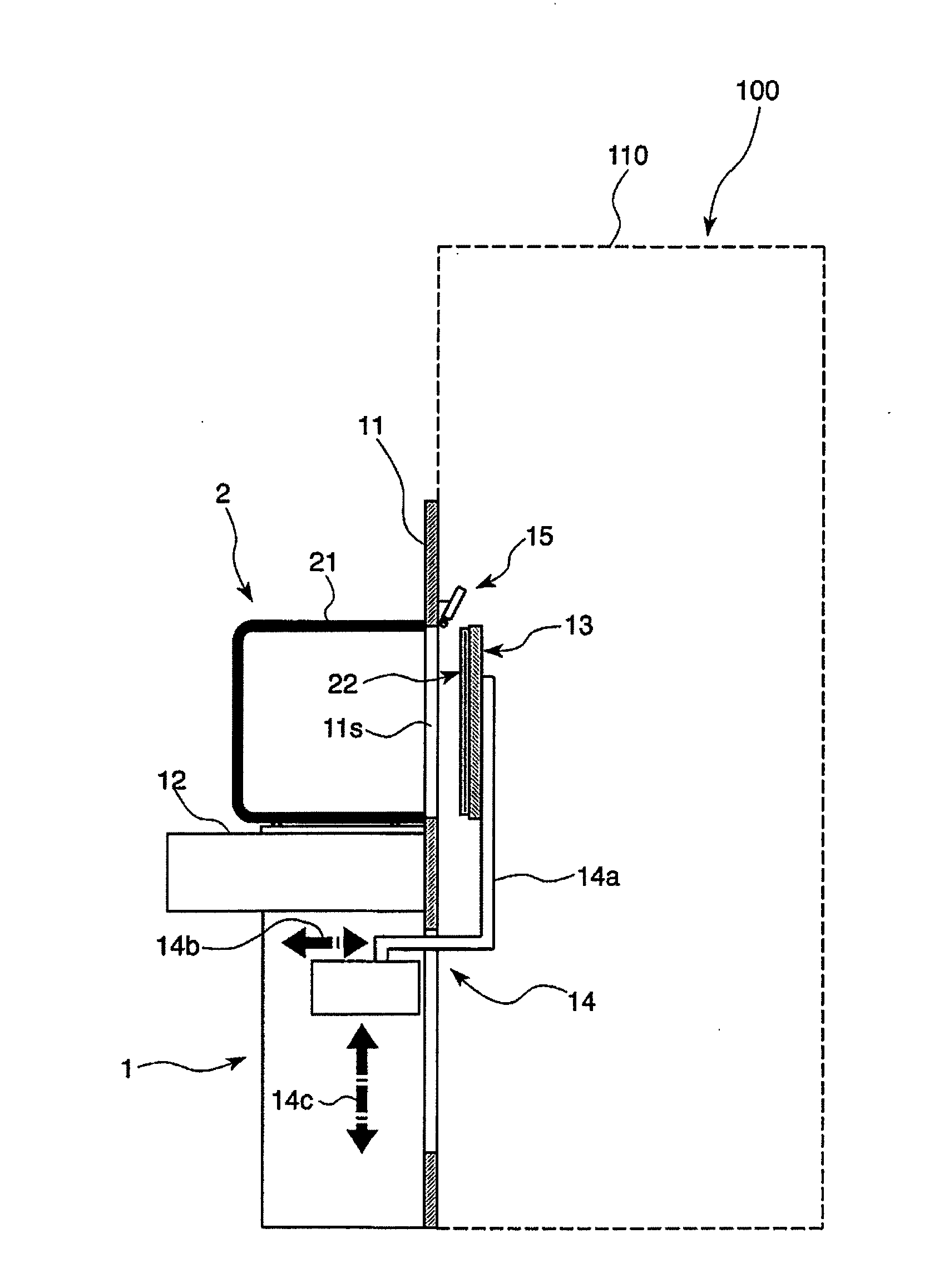
[0020]FIG. 1 schematically shows a load port 1 according to the embodiment of the present invention. Referring to FIG. 1, the load port 1 shown configures an EFEM (Equipment Front End Module) 100, which is disposed adjacent a semiconductor manufacturing apparatus not shown, together with a wafer transporting apparatus 110 in which a wafer transporting robot not shown and so forth are installed. The load port 1 functions as an interface for transferring a wafer not shown between the inside of a wafer accommodating vessel 2 and the semiconductor manufacturing apparatus. The wafer accommodating vessel 2 is configured from a vessel which complies with predetermined standards such as a FOUP (Front-Opening Unified Pod), an H-MAC (Horizontal-MAC) or a FOSB (Front Open Shipping Box). The load port 1 of the present embodiment is ready for transfer of a wafer into and from t...


PUM


Abstract

A load port including a frame having an opening, a vessel receiving table that receives the wafer vessel, a door removably attached to the opening, a door opening and closing mechanism that opens and closes the door, and a closing mechanism that exerts force on the door when the door opening and closing mechanism closes the door.

Description

CROSS REFERENCE TO RELATED APPLICATION[0001]This application claims priority to Japanese Application Number 2010-178235, filed Aug. 7, 2010, the entire contents of which are hereby incorporated by reference.BACKGROUND OF THE INVENTION[0002]1. Field of the Invention[0003]This invention relates to a load port used to transfer a wafer from and into a wafer accommodating vessel such as a FOUP (Front-Opening Unified Pod), a MAC (Multi Application Carrier) or a FOSB (Front Open Shipping Box) upon semiconductor manufacture.[0004]2. Description of the Related Art[0005]In a manufacturing process of semiconductors, a wafer is processed in a clean room in order to assure an enhanced yield and enhanced quality. However, in these days in which high integration of devices, miniaturization of circuits and increase in size of wafers have proceeded, it is difficult to manage fine dust in the inside of the overall clean room from a point of view of the cost and the technology. Therefore, as a method ...

Claims


Application Information

Patent Timeline
Patent Type & Authority Applications(United States)
IPC IPC(8): H01L21/67
CPCH01L21/67772H01L21/02H01L21/67
Inventor ASA, FUMINORITANIYAMA, YASUSHI
Owner SINFONIA TECHNOLOGY CO LTD
Features
  • R&D
  • Intellectual Property
  • Life Sciences
  • Materials
  • Tech Scout
  • Unparalleled Data Quality
  • Higher Quality Content
  • 60% Fewer Hallucinations
Learn More