Printed circuit board and method for avoiding electromagnetic interference

a printed circuit board and electromagnetic interference technology, applied in cross-talk/noise/interference reduction, printed circuit aspects, instruments, etc., can solve problems such as electromagnetic interference, disruption of operation of electronic devices, electromagnetic interference, etc., to improve the quality of the electromagnetic interference, reduce the disruption of operation, and reduce the effect of electromagnetic interferen

Inactive Publication Date: 2012-03-01
MILTOPE CORP
View PDF12 Cites 1 Cited by
  • Summary
  • Abstract
  • Description
  • Claims
  • Application Information

AI Technical Summary

Benefits of technology

[0005]Without exposed conductive traces acting as antennas in a high-voltage / meter EMC test, electromagnetic interference is drastically reduced, which is critical for many products in military and aerospace applications. Electromagnetic interference is the disruption of operation of an electronic device when the device is in the vicinity of an electromagnetic field (EM field) in the radio frequency (RF) spectrum that is caused by another electronic device. The present invention also extends the lifecycle of a product and improves its quality due to the fact that EMI susceptibility can cause damage over time.

Problems solved by technology

With this arrangement, only points, or small areas, of conductive material are on the outer surface of the outer layer and, as a result, there is insufficient material on the outer surface of the outer layer to act as antennas that absorb and re-transmit the 200-volts / meter burst of an electromagnetic compatibility (EMC) test.
Electromagnetic interference is the disruption of operation of an electronic device when the device is in the vicinity of an electromagnetic field (EM field) in the radio frequency (RF) spectrum that is caused by another electronic device.

Method used


Image

  • Printed circuit board and method for avoiding electromagnetic interference
  • Printed circuit board and method for avoiding electromagnetic interference
  • Printed circuit board and method for avoiding electromagnetic interference

Examples


Embodiment Construction

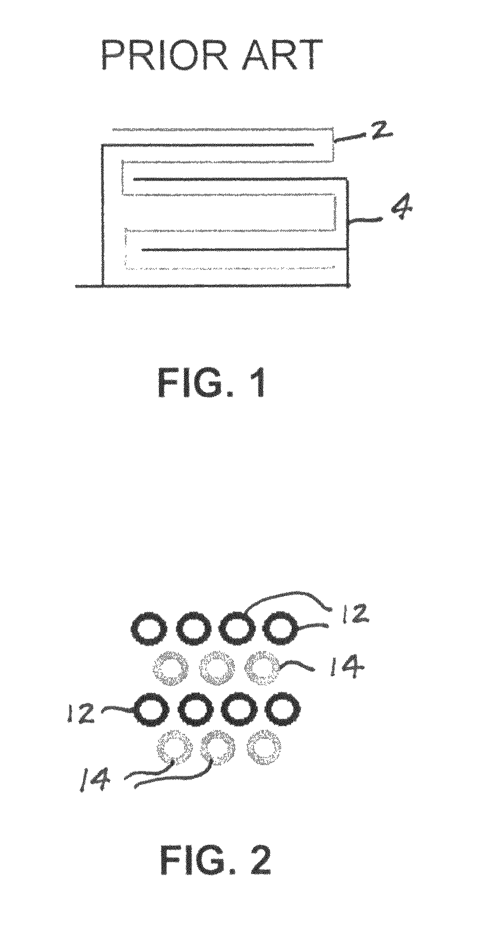
[0010]As can be seen from FIG. 1, known printed circuit boards have traces, such as a signal trace 2 and a ground trace 4, forming an outer conductive layer on an outward facing surface of an outer nonconductive layer. Such positioning of the signal traces presents electromagnetic interference issues. Typically, a matrix of such traces is provided.

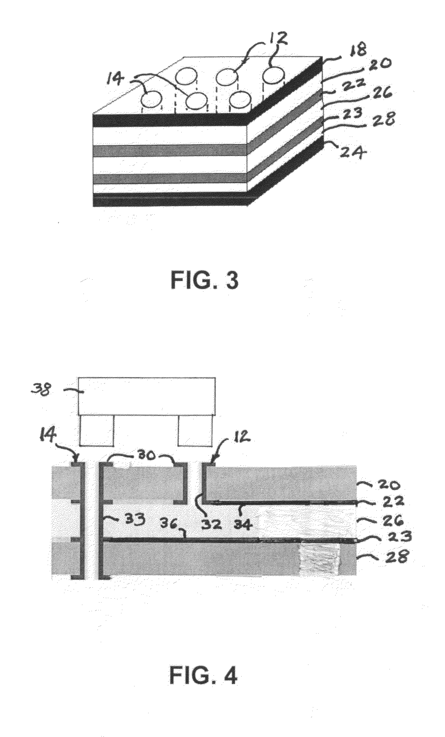
[0011]As can be seen from FIG. 2, printed circuit boards according to the present invention, rather than having signal traces on an outward facing surface of an outer nonconductive layer, have the ends of vertical interconnect accesses (vias), such as a signal via 12 and a ground via 14, on an outward facing surface of an outer nonconductive layer.

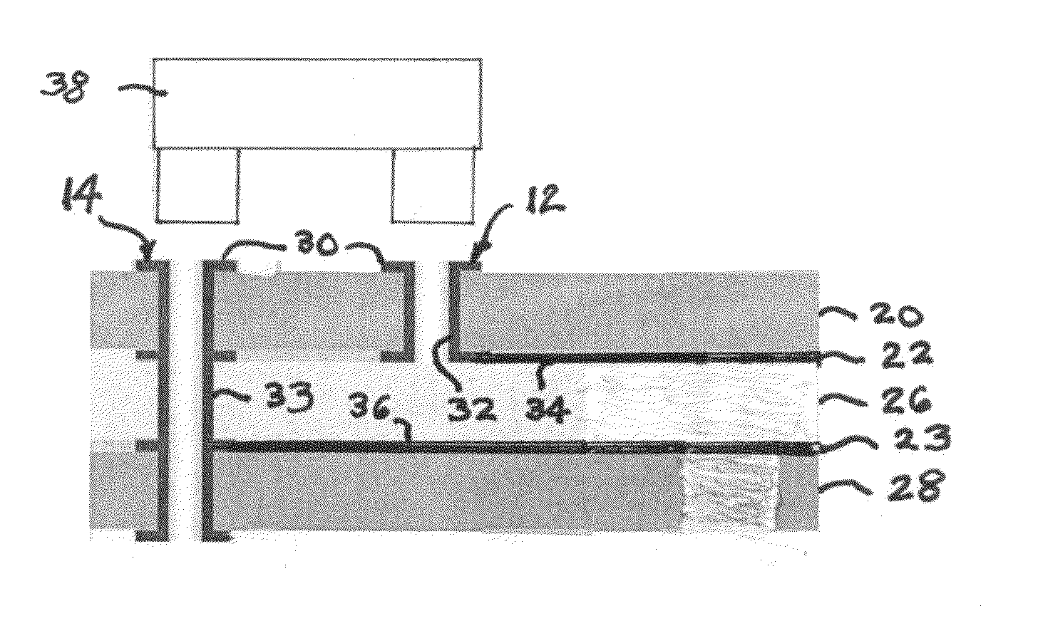
[0012]FIG. 3 shows a portion of a printed circuit board 16 having the ends of vias 12 and 14 comprising an outer conductive layer 18 positioned on an outward facing surface of an outer nonconductive layer 20. The printed circuit board 16 also includes inner conductive layers 22 and 23 and an oute...


PUM


Abstract

A printed circuit board, especially for a computer keypad, and method for avoiding electromagnetic interference include conductive signal traces positioned on a surface of one of a nonconductive layer that is other than the outward facing surface of an outer nonconductive layer, and vertical interconnect accesses extending through the outer nonconductive layer and connecting the signal traces to the outward facing surface of the outer nonconductive layer, wherein each vertical interconnect access includes a conductive portion on the outward facing surface of the outer nonconductive layer, and the conductive portion has an area no greater than 1/10 the area of the asociated signal trace. Keys selectively connect pairs of vertical interconnect accesses.

Description

BACKGROUND OF THE INVENTION[0001]The present invention relates to avoiding electromagnetic interference (EMI) involving a printed circuit board. It especially relates to avoiding electromagnetic interference involving a printed circuit board of a keyboard of a computer, particularly in military and aerospace applications.[0002]For many military computing applications, a 200 volts-per-meter electromagnetic compatibility (EMC) testing is performed. The vast susceptibility issues arising from this kind of test are a direct result of outwardly-facing conductive signal traces on the external layers of printed circuit boards (PCBs). One example is the keyboard of a laptop computer. The outer-layer signal traces can easily act as antennas that absorb and re-transmit the 200-volts / meter burst of an electromagnetic (EM) susceptibility test. This leads to a wide-ranging number of issues causing failures in the electrical system. In current designs of standard keyboards, depressing any key “sh...

Claims


Application Information

Patent Timeline
Patent Type & Authority Applications(United States)
IPC IPC(8): H01H13/76H05K1/11
CPCG06F3/0202H01H2239/004H01H2239/018H05K1/0218H05K2201/10053H05K2201/0715H05K2201/09481H05K2201/09609H05K1/115
Inventor KOTSON, MICHAELSIDLE, ERICTHAMM, GREGORY HAROLD
Owner MILTOPE CORP
Why Eureka
Try Eureka