Light-emitting device and method for manufacturing light-emitting device

a technology of light-emitting devices and manufacturing methods, which is applied in the manufacturing of semiconductor/solid-state devices, semiconductor devices, electrical devices, etc., can solve the problems of reduced wavelength conversion efficiency of fluorescent materials, large amount of fluorescent materials to be added, and inconvenient in terms of cost, so as to enhance the adhesiveness of the first sealing resin

Active Publication Date: 2012-03-01
SHARP KK
View PDF3 Cites 26 Cited by
  • Summary
  • Abstract
  • Description
  • Claims
  • Application Information

AI Technical Summary

Benefits of technology

[0030]As described above, a light-emitting device of the present invention includes a silicon oxide insulating film provided between a substrate and at least one light-emitting section, the silicon oxide insulating film being directly formed on at least an area of an upper surface of the substrate in which area the at least one light-emitting section is provided, a first sealing resin being formed directly on an upper surface of the silicon oxide insulating film so as to cover at least one light-emitting element.
[0031]A method for manufacturing the light-emitting device of the present invention includes the steps of: forming a silicon oxide insulating film directly on at least an area of the upper surface of the substrate in which area the at least one light-emitting section is to be provided, the upper surface having a wiring pattern; forming a water-repellent film on the upper surface of the substrate so as to cover the silicon oxide insulating film; forming an opening in the water-repellent film, for exposing, through the opening, the silicon oxide insulating film formed on the area in which the at least one light-emitting section is to be provided; providing the at least one light-emitting element on the silicon oxide insulating film within the opening; and forming the first sealing resin by injecting a liquid resin into the opening so as to cover the at least one light-emitting element and curing the liquid resin.
[0032]Hence, the first sealing resin is formed directly on the silicon oxide insulating film which is formed directly on the substrate. This can enhance the adhesiveness of the first sealing resin with respect to the substrate. Accordingly, the first sealing resin is hardly separated even if external stress is applied to the first sealing resin.
[0033]Further, a light-emitting device of the present invention includes: an alumina insulating film provided between the substrate and the at least one light-emitting section; and a silicon oxide insulating film provided between the substrate and the at least one light-emitting section, the alumina insulating film being formed directly on a whole area of the upper surface of the substrate, the silicon oxide insulating film being formed directly on at least an area of an upper surface of the alumina insulating film in which area the at least one light-emitting section is provided, the first sealing resin being formed directly on an upper surface of the silicon oxide insulating film so as to cover the at least one light-emitting element.
[0034]A method for manufacturing the light-emitting device of the present invention includes: the steps of: forming an alumina insulating film directly on a whole area of the upper surface of the substrate, the upper surface having a wiring pattern; forming a silicon oxide insulating film directly on at least an area of an upper surface of the alumina insulating film in which area the at least one light-emitting section is to be provided; forming a water-repellent film on the upper surface of the alumina insulating film so as to cover the silicon oxide insulating film; forming an opening in the water-repellent film, for exposing, through the opening, the silicon oxide insulating film formed on the area in which the at least one light-emitting section is to be provided; providing the at least one light-emitting element on the silicon oxide insulating film within the opening; and forming the first sealing resin by injecting a liquid resin into the opening so as to cover the at least one light-emitting element and curing the liquid resin.
[0035]Hence, the first sealing resin is formed directly on the silicon oxide insulating film, and the silicon oxide insulating film is formed directly on the alumina insulating film which is formed directly on the substrate. This can enhance the adhesiveness of the first sealing resin with respect to the substrate. Accordingly, the first sealing resin is hardly separated even if external stress is applied to the first sealing resin.

Problems solved by technology

Gathering of the fluorescent material into the top of the sealing resin means that the fluorescent material is away from the light-emitting element, resulting in reduction in wavelength conversion efficiency of the fluorescent material.
Therefore, a large amount of fluorescent material needs to be added, but this is not preferable in terms of cost.
However, this causes a lot of problems, for example, complication of a molding machine.
However, in the aforementioned sealing method, the dam sheet is thrown away every time when sealing is finished.
Therefore, this sealing method disadvantageously highly costs.

Method used


Image

  • Light-emitting device and method for manufacturing light-emitting device
  • Light-emitting device and method for manufacturing light-emitting device
  • Light-emitting device and method for manufacturing light-emitting device

Examples


embodiment 1

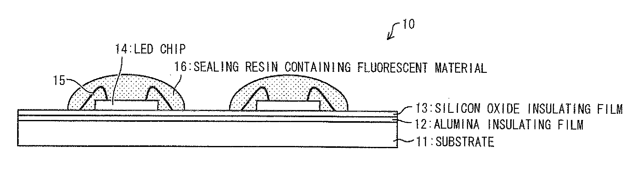
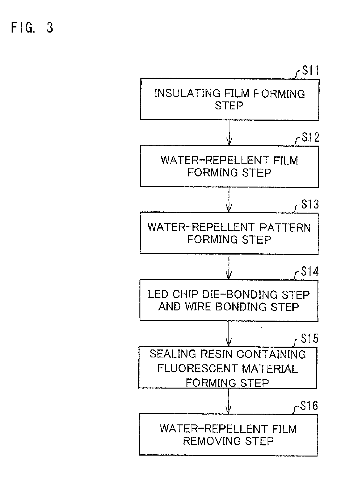
[0050]An embodiment of the present invention will be described below with reference to the drawings. In this embodiment, there will be described a light-emitting device usable as a light source of a lighting device, a display device, or the like. Note that, in the description below, upper and lower sides of FIG. 1 correspond to upper and lower sides of the light-emitting device, respectively.

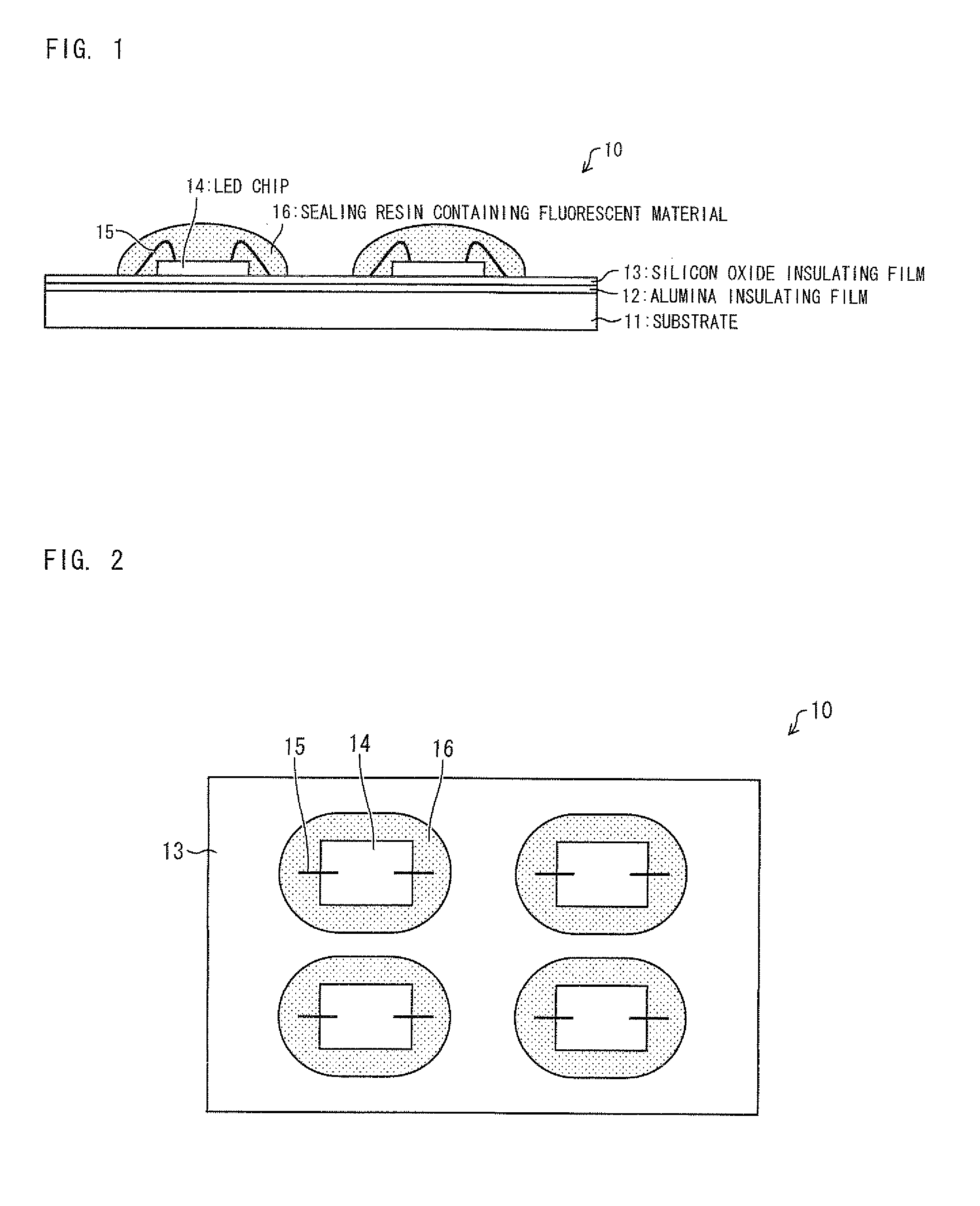
[0051]FIG. 1 is a sectional view showing a structural example of a light-emitting device 10 according to this embodiment. FIG. 2 is a plan view of the light-emitting device 10. As shown in FIG. 1 and FIG. 2, the light-emitting device 10 includes a substrate 11, an alumina insulating film 12, a silicon oxide insulating film 13, LED chips (light-emitting elements) 14, and a sealing resin containing fluorescent material (first sealing resin) 16. Note that, in FIG. 2, a part of the sealing resin 16 containing fluorescent material is shown transparently in order to show the LED chips 14 clearly.

[0052...

embodiment 2

[0101]Another embodiment of the present invention will be described below with reference to the drawings. Note that, a structure that is not described in this embodiment is the same as in Embodiment 1. Further, for the sake of easy explanation, members having the like functions as the members in the drawings of Embodiment 1 are denoted by the like symbols and the detailed description thereof is omitted.

[0102]FIG. 12 is a sectional view of a structural example of a light-emitting device 20 of this embodiment. As shown in FIG. 12, the light-emitting device 20 includes light-transmitting resin domes (second sealing resin) 21 and a light-transmitting resin layer 22 in addition to the structure of the light-emitting device 10 of Embodiment 1. The light-emitting device 20 is a light-emitting device having a so-called dual seal structure in which LED chips 14 are sealed with two layers of resin.

[0103]Each of the light-transmitting resin domes 21 and the light-transmitting resin layer 22 is...


PUM


Abstract

A light-emitting device includes: a substrate; a light-emitting section provided on an upper surface of the substrate, the light-emitting section including an LED chip and a sealing resin containing fluorescent material covering the LED chip; and a silicon oxide insulating film provided between the substrate and the light-emitting section, the silicon oxide insulating film being formed directly on an upper surface of the substrate or an alumina insulating film, the sealing resin containing fluorescent material formed directly on an upper surface of the silicon oxide insulating film so as to cover the LED chip. Thus, this invention provides the light-emitting device capable of making the sealing resin difficult to be separated from the substrate and a method for manufacturing the light-emitting device.

Description

[0001]This Nonprovisional application claims priority under 35 U.S.C. §119(a) on Patent Application No. 2010-188164 filed in Japan on Aug. 25, 2010, the entire contents of which are hereby incorporated by reference.TECHNICAL FIELD[0002]The present invention relates to a light-emitting device including a light-emitting element (semiconductor light-emitting element) which is provided on a substrate and is covered with a sealing resin and a method for manufacturing the light-emitting device, and more particularly, relates to a technique for making a sealing resin difficult to be separated from a substrate.BACKGROUND ART[0003]A light emitting diode (LED), whose efficiency has been improved in recent years, has been widely used in a backlight of a display device and lighting equipment as a light source capable of saving more power than a light bulb or a fluorescent. Various light-emitting devices including light-emitting elements such as the LEDs have been proposed so far. In particular,...

Claims


Application Information

Patent Timeline
Patent Type & Authority Applications(United States)
IPC IPC(8): H01L33/50H01L33/52
CPCH01L25/0753H01L33/54H01L2933/0041H01L2933/005H01L2224/45144H01L2224/48091H01L2924/00014H01L2924/00
Inventor YOSHIZUMI, NOBUYUKIYAMAGUCHI, SHINJI
Owner SHARP KK
Why Eureka
Try Eureka