Phosphor film, method of forming the same, and method of coating phosphor layer on LED chips

Active Publication Date: 2012-03-01
SAMSUNG ELECTRONICS CO LTD
View PDF9 Cites 74 Cited by
  • Summary
  • Abstract
  • Description
  • Claims
  • Application Information

AI Technical Summary

Benefits of technology

[0027]The method may further include irradiating ultraviolet rays to re

Problems solved by technology

In addition, when the phosphor coating is performed on a separate chip in

Method used


Image

  • Phosphor film, method of forming the same, and method of coating phosphor layer on LED chips
  • Phosphor film, method of forming the same, and method of coating phosphor layer on LED chips
  • Phosphor film, method of forming the same, and method of coating phosphor layer on LED chips

Examples


Embodiment Construction

[0046]Reference will now be made in detail to embodiments, examples of which are illustrated in the accompanying drawings, wherein like reference numerals refer to like elements throughout and the sizes or thicknesses of the elements may be enlarged for clarity. In this regard, the present embodiments may have different forms and should not be construed as being limited to the descriptions set forth herein. Accordingly, the embodiments are merely described below, by referring to the figures, to explain aspects of the present description.

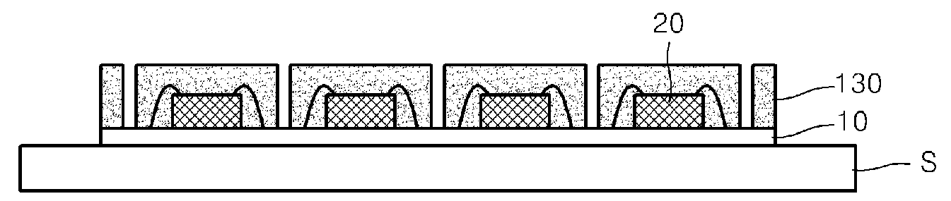
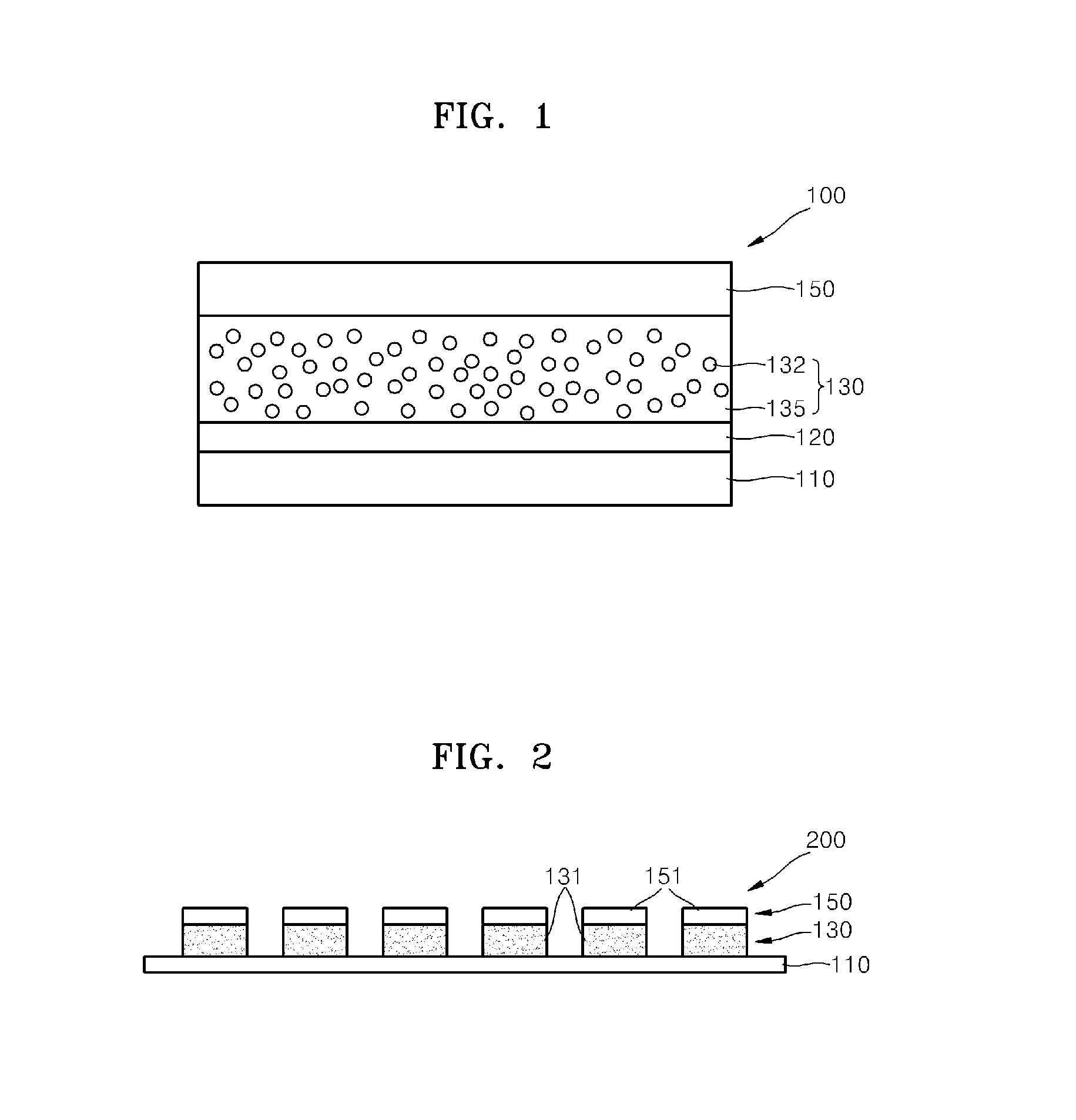
[0047]FIG. 1 is a schematic sectional view of a phosphor film 100 according to an embodiment of the present invention. Referring to FIG. 1, the phosphor film 100 may include a base film 110, a phosphor layer 130 formed on the base film 110, and a cover film 150 for protecting the phosphor layer 130. Also, a temporary adhesive layer may be further formed between the base film 110 and the phosphor layer 130.

[0048]The base film 110 may act as a carrier ...


PUM

PropertyMeasurementUnit
Temperatureaaaaaaaaaa

Abstract

Phosphor films, methods of forming the phosphor films, and methods of coating a phosphor layer on light-emitting chips are disclosed. The phosphor film includes: a base film; a phosphor layer that is formed on the base film and comprises an incompletely cured resin material and phosphor particles mixed with the incompletely cured resin material; and a cover film that is formed on the phosphor layer and protects the phosphor layer.

Description

CROSS-REFERENCE TO RELATED APPLICATIONS[0001]This application claims the benefit of Korean Patent Application No. 10-2010-0082640, filed on Aug. 25, 2010, in the Korean Intellectual Property Office, the disclosure of which is incorporated herein in its entirety by reference.BACKGROUND[0002]1. Field[0003]The present disclosure relates to a phosphor film, a method of forming the same, and a method of coating a phosphor layer on light-emitting chips.[0004]2. Description of the Related Art[0005]Light emitting diodes (LEDs) are semiconductor devices that produce light of various colors from a light emitting source formed at a PN junction of a compound semiconductor. Recently, blue LEDs and ultraviolet (UV) LEDs have been developed by using nitrides with excellent physical and chemical properties, and also, white light or light of other mono-color has been generated by using blue or UV LEDs and a phosphor material, thereby widening the application range of LEDs.[0006]Conventionally, a LED...

Claims


Application Information

Patent Timeline
IPC IPC(8): H01L33/44B32B27/00B05D5/06B32B19/00
CPCC09K11/06Y10T428/24802B32B27/00H01L2933/0041B32B19/00H01L33/505B05D5/06H01L2224/48091Y10T428/24942B32B3/10Y10T428/24893B32B5/16Y10T428/24851H01L33/50H01L2924/00014B32B7/12B32B9/04B32B9/045B32B27/06B32B27/08B32B27/32B32B3/08B32B3/14B32B3/16B32B3/18B32B2250/03B32B2250/40B32B2250/44B32B2266/025B32B2307/40B32B2307/422B32B2457/00H01L2224/45139Y10T428/31855H01L2924/00011H01L2924/00H01L2924/01049
Inventor YOO, CHEOL-JUNHONG, SEONG-JAE
Owner SAMSUNG ELECTRONICS CO LTD
Why Eureka
Try Eureka