Pitch reduction using oxide spacer

a technology of oxide spacers and semiconductor devices, which is applied in the field of semiconductor device pitch reduction, can solve the problems of high temperature, adverse to the semiconductor device, and the precision of overlaying of double mask methods is limited

Inactive Publication Date: 2012-03-01
LAM RES CORP
View PDF6 Cites 182 Cited by
  • Summary
  • Abstract
  • Description
  • Claims
  • Application Information

AI Technical Summary

Problems solved by technology

However, as the packing density increases, the cost increase and the yield reduction are also exponentially increasing.
However, the double mask method it is limited by precision of overlaying.
Such high temperatures may be detrimental to the semiconductor device.
The h...

Method used


Image

  • Pitch reduction using oxide spacer
  • Pitch reduction using oxide spacer
  • Pitch reduction using oxide spacer

Examples


Embodiment Construction

[0017]The present invention will now be described in detail with reference to a few preferred embodiments thereof as illustrated in the accompanying drawings. In the following description, numerous specific details are set forth in order to provide a thorough understanding of the present invention. It will be apparent, however, to one skilled in the art, that the present invention may be practiced without some or all of these specific details. In other instances, well known process steps and / or structures have not been described in detail in order to not unnecessarily obscure the present invention.

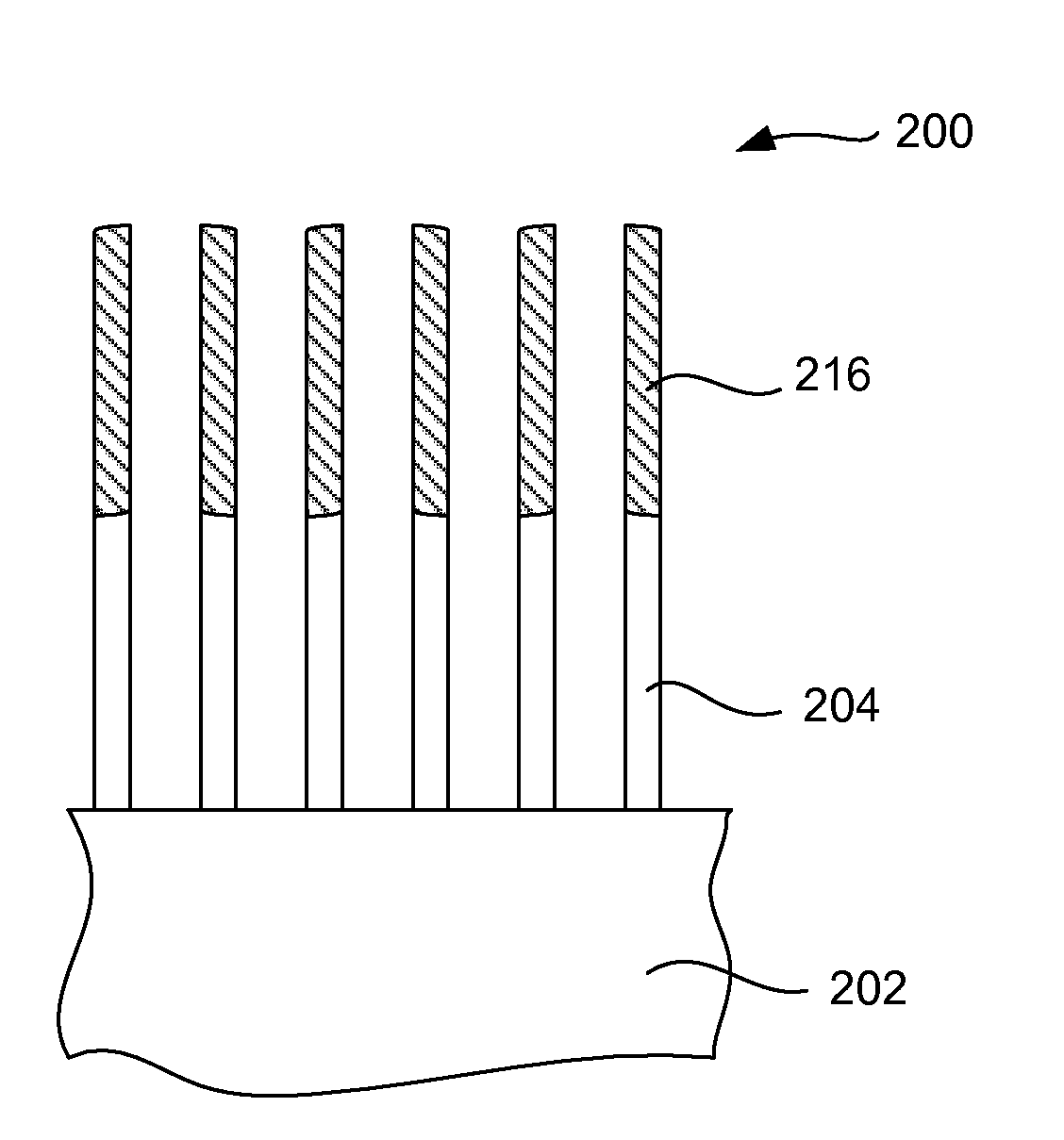
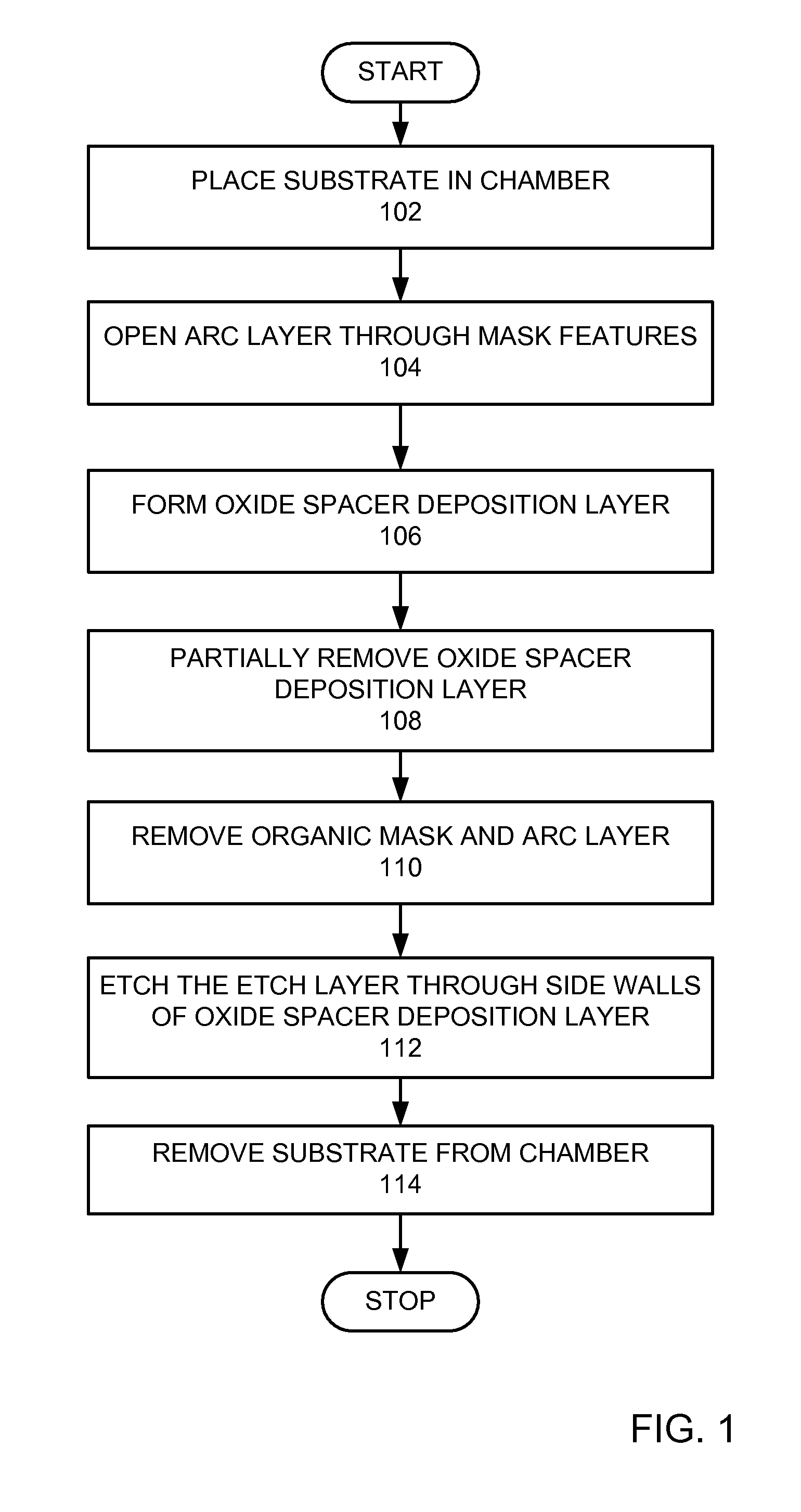
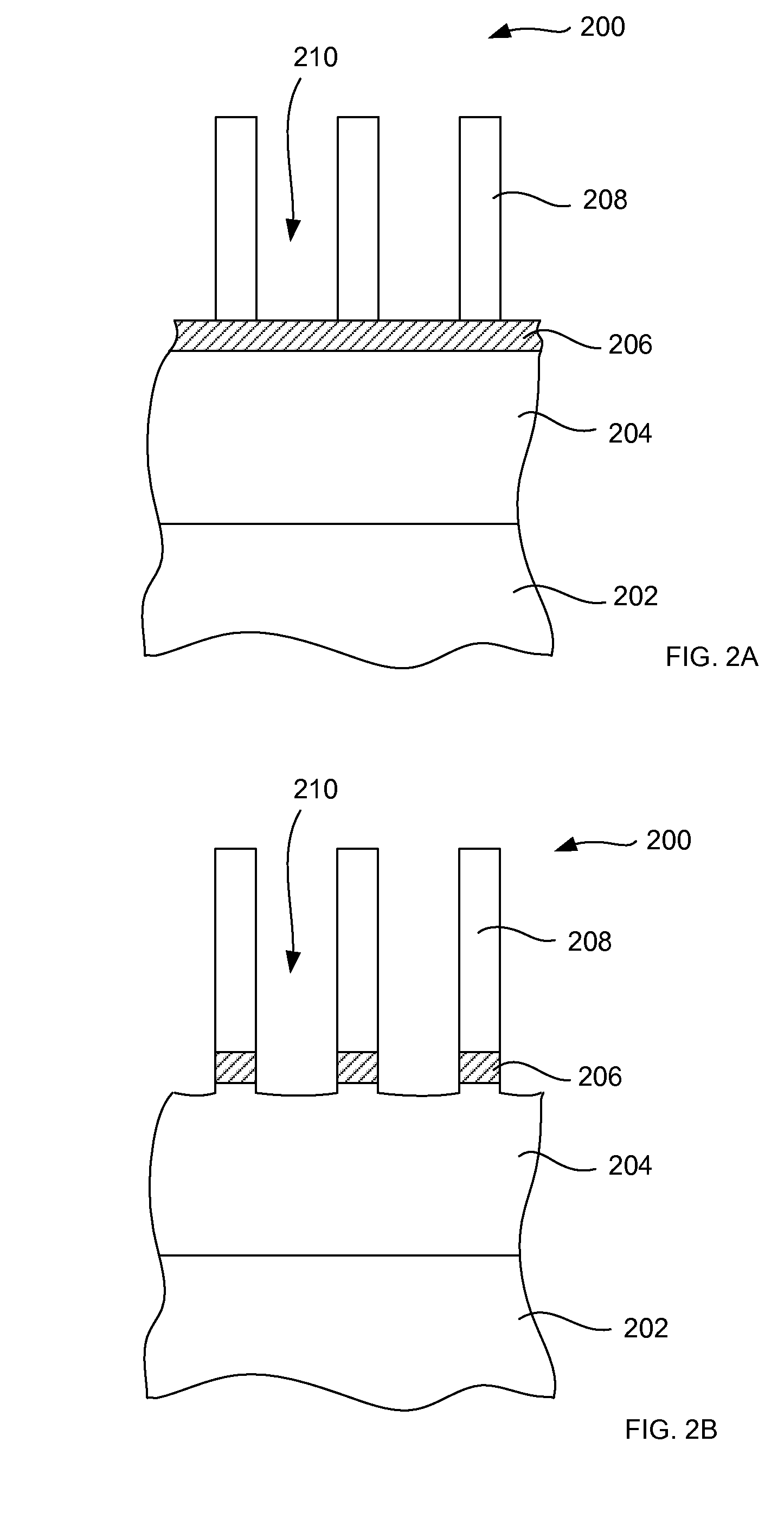
[0018]To facilitate understanding, FIG. 1 is a high level flow chart of a process that may be used in an embodiment of the invention, which etches an etch layer disposed over a substrate and below an antireflective coating (ARC) layer and a patterned organic mask with mask features. A substrate is placed in a process chamber (step 102). FIG. 2A is a schematic cross-sectional view of a stac...


PUM

PropertyMeasurementUnit
Temperatureaaaaaaaaaa

Abstract

A method for etching an etch layer disposed over a substrate and below an antireflective coating (ARC) layer and a patterned organic mask with mask features is provided. The substrate is placed in a process chamber. The ARC layer is opened. An oxide spacer deposition layer is formed. The oxide spacer deposition layer on the organic mask is partially removed, where at least the top portion of the oxide spacer deposition layer is removed. The organic mask and the ARC layer are removed by etching. The etch layer is etched through the sidewalls of the oxide spacer deposition layer. The substrate is removed from the process chamber.

Description

BACKGROUND OF THE INVENTION[0001]The present invention relates to the formation of semiconductor devices. More particularly, the invention relates to the formation of semiconductor devices with pitch reduction using oxide spacers.[0002]The packing density of semiconductor devices may increase twice by about every one and half year. The high packing density increases productivity and device speed and also reduces power consumption. However, as the packing density increases, the cost increase and the yield reduction are also exponentially increasing. Since the largest cause of exponential increase of cost and yield reduction may be related to the lithography technology, alternative methods for patterning a mask have been sought to replace optical lithography. One such technology is the double mask scheme which patterns the mask layer twice to make half pitch. However, the double mask method it is limited by precision of overlaying.[0003]In general, spacer lithography provides a sacrif...

Claims


Application Information

Patent Timeline
IPC IPC(8): H01L21/302B23K10/00
CPCH01L21/02337H01L21/0228H01L21/31654H01L21/02126H01L21/31144H01L21/31612H01L21/0338H01L21/02211H01L21/0234H01L21/02274H01L21/0337H01L21/32139
Inventor KIM, JISOOCHIANG, CONANSHINAGAWA, JUNSADJADI, S.M. REZA
Owner LAM RES CORP
Why Eureka
Try Eureka