High Dynamic Range CMOS Pixel and Method of Operating Same

a high-dynamic range, cmos pixel technology, applied in the field of imaging devices, can solve problems such as limited dynamic range, and achieve the effect of increasing the magnitude of the potential, and increasing the size of the potential barrier

Inactive Publication Date: 2012-03-08
LEVINE PETER ALAN +1
View PDF4 Cites 14 Cited by
  • Summary
  • Abstract
  • Description
  • Claims
  • Application Information

AI Technical Summary

Benefits of technology

[0013]In an embodiment, increasing the size of the potential barrier may include increasing a magnitude of a potential applied to the transfer gate from a first level before the first integration time to a second level at the second integration time. The size of the potential barrier may be increased non-linearly as a function of time. The size of the potential barrier may increased in discrete steps over time or continuously over time. The second ...

Problems solved by technology

Thus, dynami...

Method used


Image

  • High Dynamic Range CMOS Pixel and Method of Operating Same
  • High Dynamic Range CMOS Pixel and Method of Operating Same
  • High Dynamic Range CMOS Pixel and Method of Operating Same

Examples


Embodiment Construction

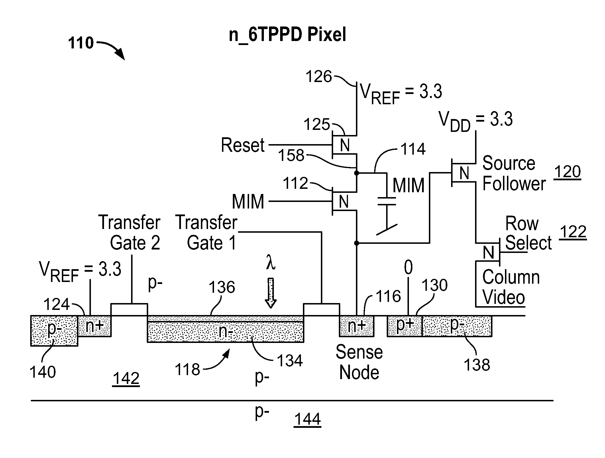
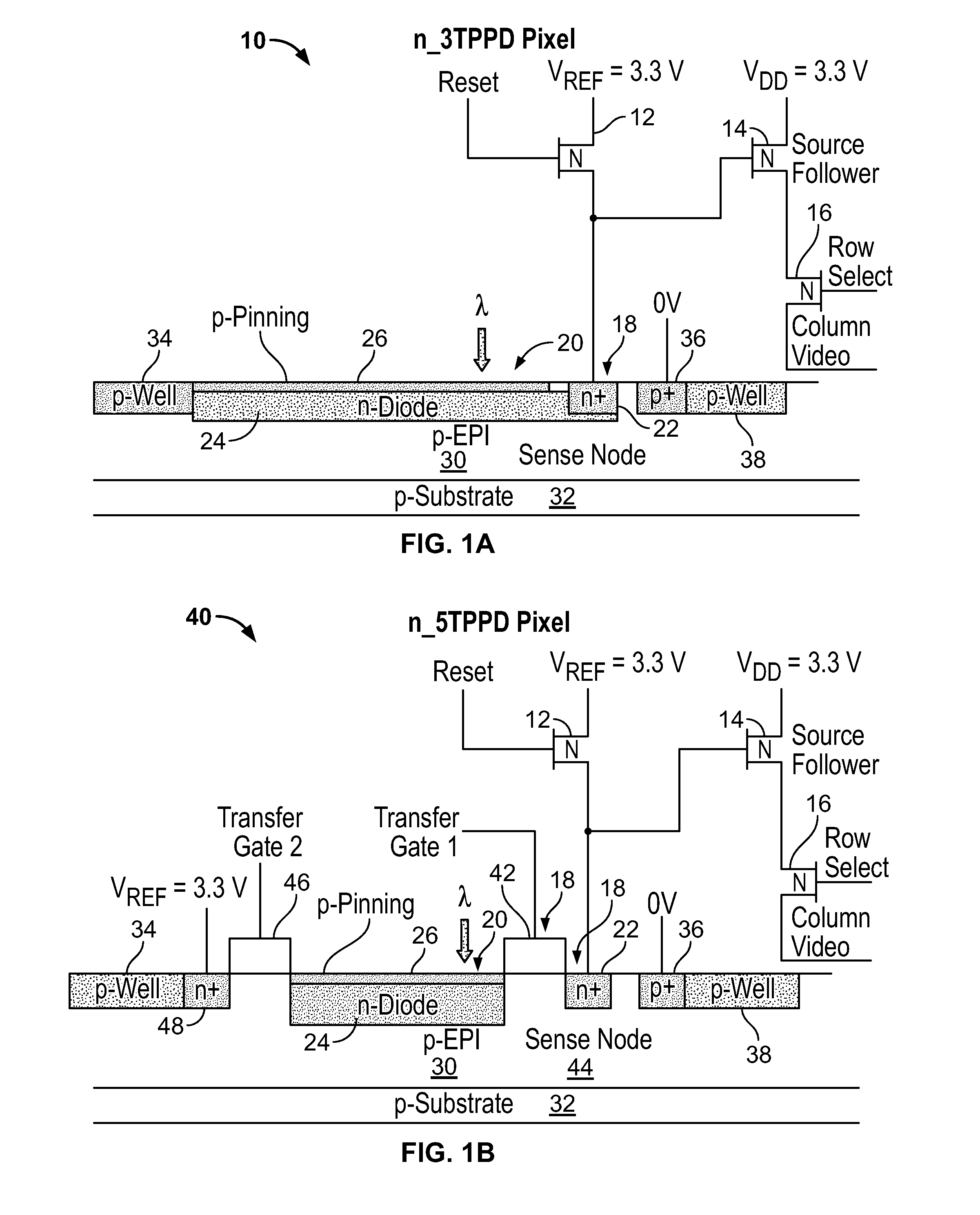
[0028]Referring again to FIG. 1B, according to an embodiment of the present invention, the 5T pixel 40 may operate with high dynamic range by an incremental skimming of photocharge from the PPD 24. This improves optical dynamic range by partial removal of overload charge. The light level falling on the PPD 24 may exceed a value that would normally overfill the charge capacity of the pinned photodiode 24. In the following discussion, TRANSFER GATE 2 is used as an example. TRANSFER GATE 2, in conjunction with the potential 54 below the PPD 24, may be manipulated to produce a nonlinear response. More particularly, the potential of TRANSFER GATE 2 in the region 54 may be manipulated to control charge capacity of the PPD 24.

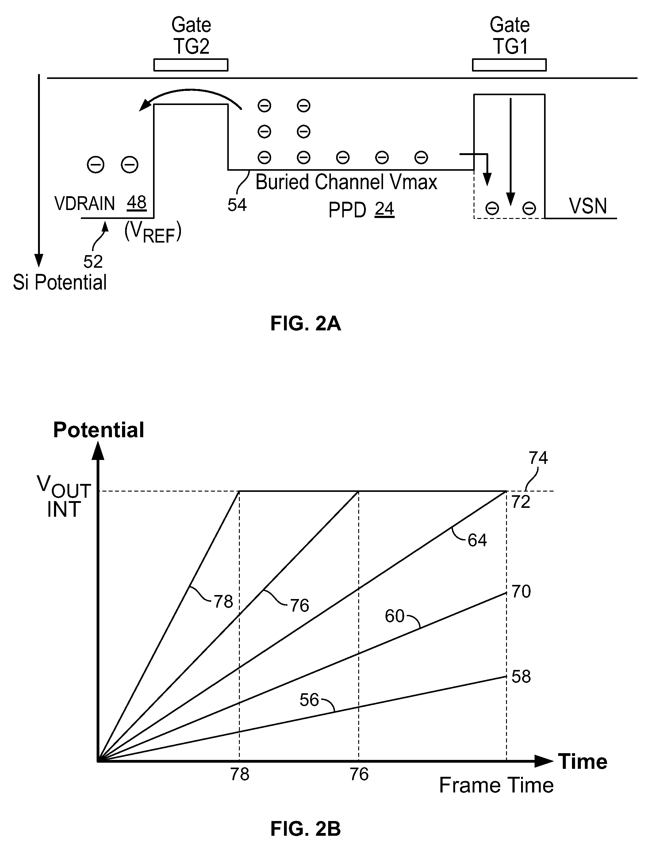
[0029]FIGS. 3A and 3B are a potential diagram depicting a method of modulating voltage applied to TRANSFER GATE 1 or 2 to increase the charge capacity of the PPD 26, according to an embodiment of the present invention. Referring now to FIGS. 1B and 3A, initially, the ...


PUM


Abstract

A method of operating a CMOS pixel is disclosed. The CMOS pixel includes a photodiode (PPD), a transfer gate coupled to the PPD, and an anti-blooming drain coupled to the transfer gate. A potential barrier is formed between a potential well underlying the PPD and the transfer gate. Charge is accumulated in the potential well in response to electromagnetic radiation during a first integration time. Excess charge is removed from the potential well to the anti-blooming drain that exceeds the first potential barrier. A size of the potential barrier is increased. Charge is accumulated in the potential well during a second integration time.

Description

CROSS-REFERENCES TO RELATED APPLICATIONS[0001]This application is a continuation of U.S. utility application No. 13 / 223,991 filed Sep. 1, 2011, which claims the benefit of U.S. provisional patent application No. 61 / 379,504 filed Sep. 2, 2010, the disclosures of which are incorporated herein by reference in their entirety.FIELD OF THE INVENTION[0002]The invention relates generally to imaging devices. More specifically, the invention relates to improving the dynamic range of CMOS pixels.BACKGROUND OF THE INVENTION[0003]CMOS image sensors first came to the fore in relatively low-performance applications where shuttering was not required, scene dynamic range was low, and moderate to high noise levels could be tolerated. A CMOS sensor technology enabling a higher level of integration of an image array with associated processing circuits would be beneficial to many digital applications such as, for example, in cameras, scanners, machine vision systems, vehicle navigation systems, video te...

Claims


Application Information

Patent Timeline
IPC IPC(8): G01J1/42
CPCH04N5/3592H04N25/622
Inventor LEVINE, PETER ALANZHU, RUI
Owner LEVINE PETER ALAN
Why Eureka
Try Eureka