Printing material cartridge and printing material supply system

a technology of printing material and printing cartridge, which is applied in the direction of printing, etc., can solve the problems of undesired high voltage applied to failure of the circuitry and the possibility of failure or insufficient connection between the plurality of terminals of the printing material cartridge and those of the printing apparatus, so as to reduce the possibility of failur

Active Publication Date: 2012-03-08
SEIKO EPSON CORP
View PDF1 Cites 73 Cited by
  • Summary
  • Abstract
  • Description
  • Claims
  • Application Information

AI Technical Summary

Benefits of technology

[0009]An object of the invention is to provide a technique that enables a printing material cartridge to be attached in an adequately correct orientation or alignment. It is also desired to provide a technique that reduces the possibility of failure by application of an unexpectedly high voltage to the circuitry of the printing material cartridge.

Problems solved by technology

Especially with recent size reduction of the individual terminals, there is an increased possibility of failed or insufficient connection between the plurality of terminals of the printing material cartridge and those of the printing apparatus, due to inadequate orientation or alignment of the printing material cartridge.
In the course of attachment of the printing material cartridge, there is a possibility that an undesired high voltage is applied to the circuitry on the printing material cartridge.
Application of the undesired high voltage to the circuitry on the printing material cartridge may cause a failure in the circuitry on the printing material cartridge.
Adhesion of dust or ink may cause a short circuit between the high voltage terminal and the low voltage terminal and lead to apply an undesired high voltage to the low voltage terminal.
In the actual state, however, small clearances are present between the contact portions on the circuit board and the terminals on the printing apparatus and their peripheries and tend to suck the ink by capillarity.
When the contact portions on the circuit board adapted to contact with the terminals on the printing apparatus, the friction-induced static electricity tends to suck the dust.
In the above arrangement, when dust or ink adheres across the high voltage terminal and the low voltage terminal, there is a high probability that the adhesion area of dust or ink includes the terminal for overvoltage detection.
There is, however, a high probability that the adhesion area of such long, thin dust includes the ground terminal.
As discussed above, even when dust or ink adheres to the circuit board in any state, the arrangement may prevent the circuitry from being damaged, or prevent the memory device from being damaged when the low voltage terminal is connected with the memory device, by application of an undesired high voltage, with significantly high probability.
Adhesion of dust or ink may cause a short circuit between the high voltage terminal and the low voltage terminal and lead to apply an undesired high voltage to the low voltage terminal.
In the actual state, however, small clearances are present between the contact portions and the terminals on the printing apparatus and their peripheries and tend to suck the ink by capillarity.
When the contact portions come into contact with the terminals on the printing apparatus, the friction-induced static electricity tends to suck the dust.
In the above arrangement, when dust or ink adheres across the high voltage terminal and the low voltage terminal, there is a high probability that the adhesion area of dust or ink includes the terminal for overvoltage detection.
There is, however, a high probability that the adhesion area of such long, thin dust includes the ground terminal.
As discussed above, even when dust or ink adheres to the circuit board in any state, the arrangement may prevent the circuitry from being damaged, or prevent the memory device from being damaged when the low voltage terminal is connected with the memory device, by application of an undesired high voltage, with significantly high probability.

Method used


Image

  • Printing material cartridge and printing material supply system
  • Printing material cartridge and printing material supply system
  • Printing material cartridge and printing material supply system

Examples


first embodiment

A. First Embodiment

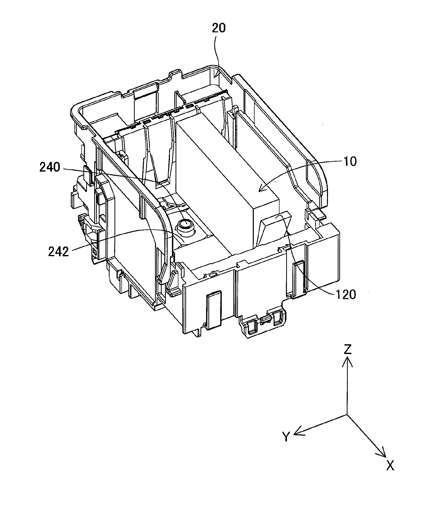
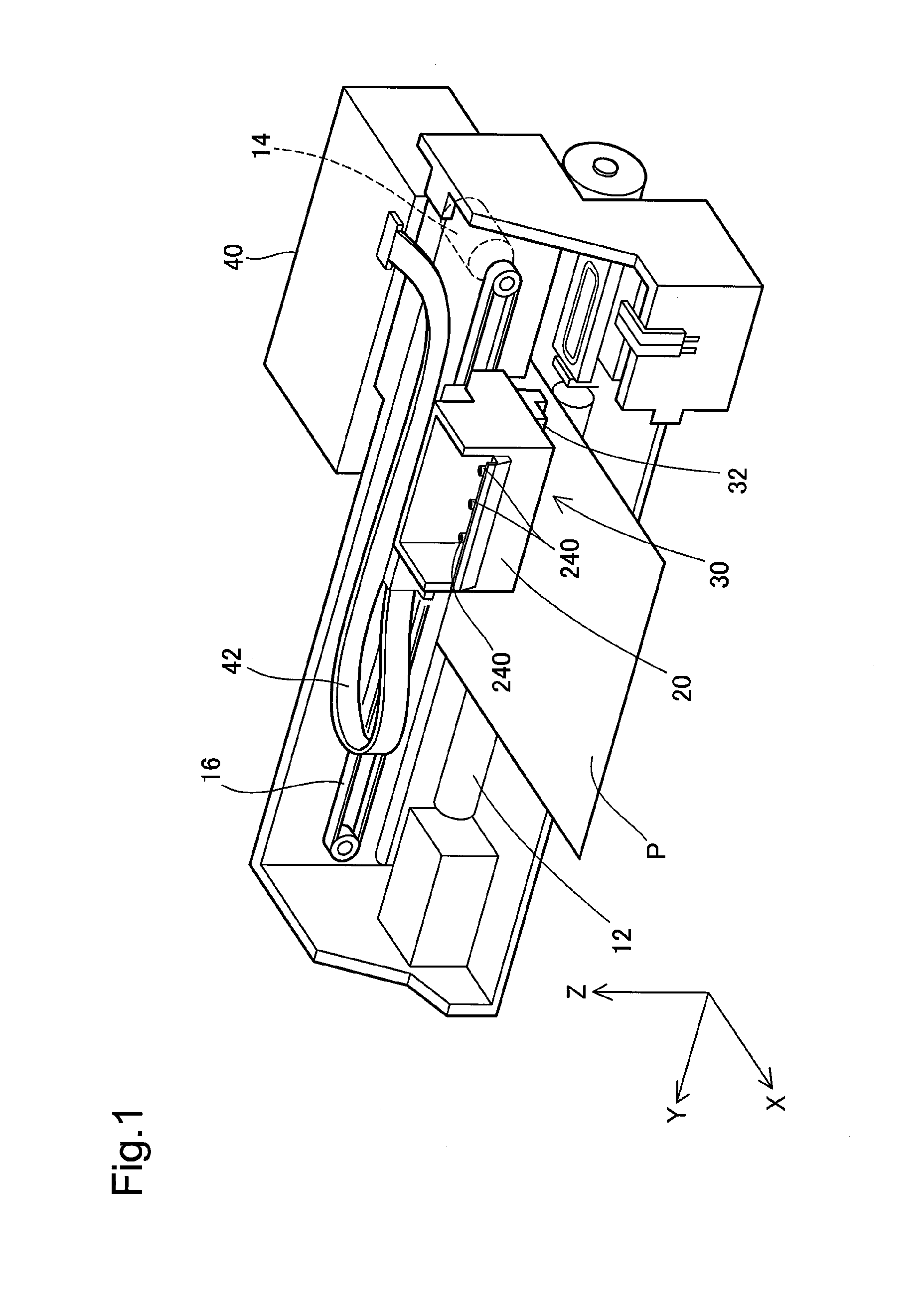
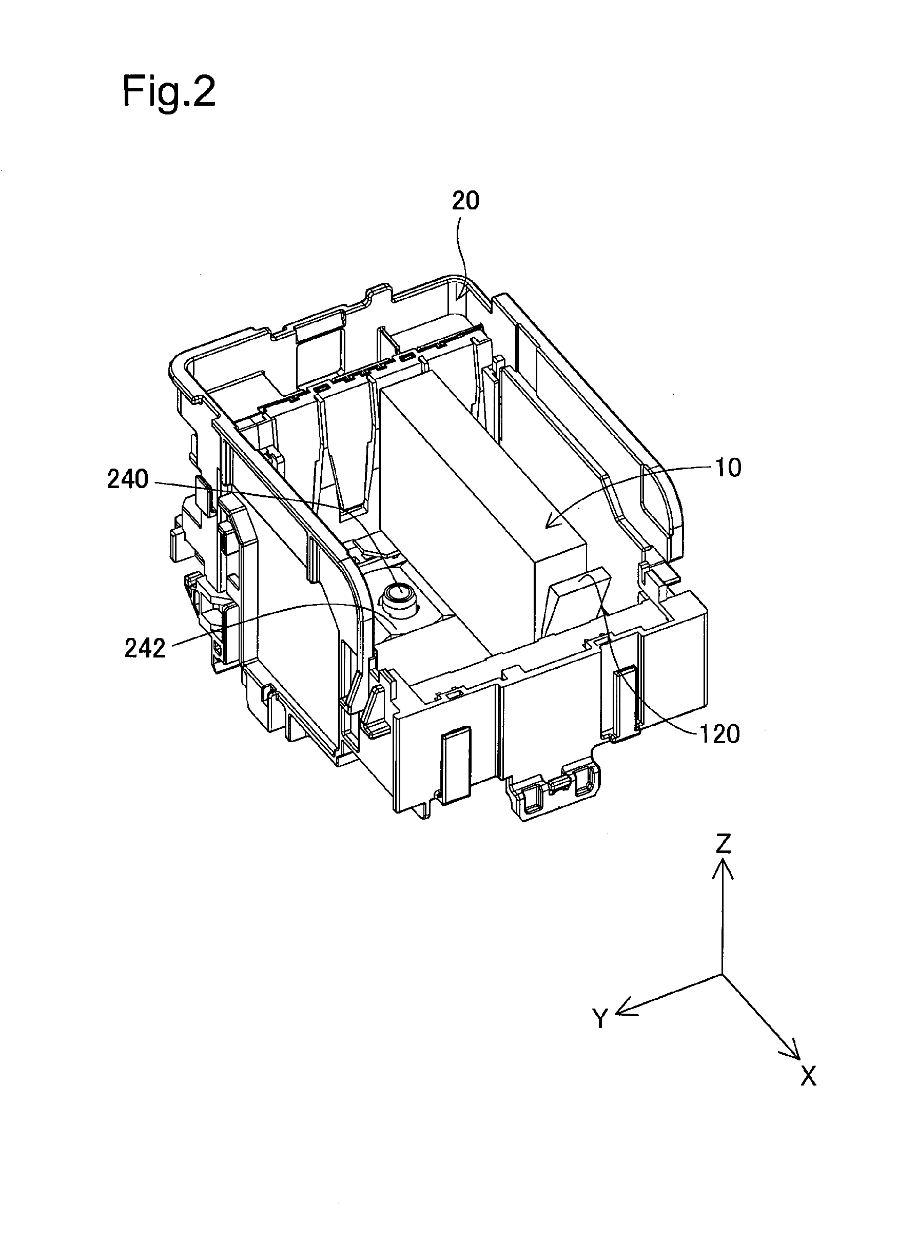
[0091]FIG. 1 is a perspective view showing the structure of a printing apparatus according to a first embodiment of the invention. FIG. 1 includes indication of XYZ axes that are orthogonal to one another. The XYZ axes in FIG. 1 correspond to the XYZ axes in the other drawings. Some of the subsequent drawings also include similar indication of the XYZ axes. In this embodiment, when the printing apparatus is in a position in use, the Z-axis direction is the vertical direction, and a face in the X-axis direction of the printing apparatus forms the front face. This printing apparatus is a small-sized inkjet printer for personal use and has a sub-scan feed mechanism, a main scan feed mechanism, and a head drive mechanism. The sub-scan feed mechanism includes a paper feed roller 12, which is driven by a paper feed motor (not shown), to feed a sheet of printing paper P in a sub-scanning direction. The main scan feed mechanism includes a carriage motor 14 to move back an...

second embodiment

B. Second Embodiment

[0179]FIG. 17 shows the structure of a holder 20a according to a second embodiment. The general structure of the printing apparatus and the structure of the ink cartridge 10 of the second embodiment are the same with those of the first embodiment. FIG. 17 shows the state in the middle of insertion of the cartridge 10 to the holder 20a. A pair of longitudinal guide members 610 (first sub-guide members) and a pair of lateral guide members 620 (second sub-guide members) are provided, in addition to the fitting rib 270, in the vicinity of a terminal block 500a located in each slot of the holder 20a. As discussed above in the first embodiment, the fitting rib 270 also serves as the guide member to guide the cartridge 10.

[0180]The pair of lateral guide members 620 are located such that the inner surfaces of the pair of lateral guide members 620 are in contact with the outer surfaces of the pair of lateral guide wall members 184 of the cartridge 10 (FIG. 3). In the proc...

modification 1

[0218]The above embodiments regard the application of the invention to the on-carriage type printing apparatus which has a holder (cartridge attachment section) on the carriage. The invention may also be applicable to the off-carriage type printing apparatus which has a holder (cartridge attachment section) on the location other than the carriage.


PUM


Abstract

A printing apparatus has a cartridge attachment section including a terminal block having apparatus-side terminals disposed on its inclined surface, and a printing material supply pipe. Among the apparatus-side terminals, one apparatus-side ground terminal located on their center in Y direction is protruded to a greater height than the other plural apparatus-side terminals. A printing material cartridge has a circuit board, a printing material supply port, and a board mount portion that is inclined at an acute angle relative to a plane extended from an opening face of the printing material supply port. The circuit board is arranged such that one cartridge-side terminal on the circuit board comes into contact with the apparatus-side ground terminal prior to the other cartridge-side terminals in the process of attachment of the printing material cartridge to the cartridge attachment section. This arrangement enables the printing material cartridge to be attached in an adequate correct orientation or alignment to the printing apparatus. This arrangement also reduces the possibility of failure caused by application of a high voltage to the circuitry of the printing material cartridge.

Description

CROSS-REFERENCE TO RELATED APPLICATIONS[0001]The present application claims the priority based on Japanese Patent Application No. 2010-197320 filed on Sep. 3, 2010, the disclosure of which is hereby incorporated by reference in its entirety.BACKGROUND[0002]1. Technical Field[0003]The present invention relates to a printing material cartridge and a printing material supply system including the printing material cartridge and a printing apparatus.[0004]2. Related Art[0005]Some recent printing material cartridges have a circuit (circuit element), such as a memory device for storing information about a printing material (for example, remaining amount of ink). See JP-A-2003-011390, JP-A-2007-230249, and JP-A-2005-144723, for example. Upon attachment of the printing material cartridge to a printing apparatus, a plurality of terminals on the printing material cartridge adapted to contact with a plurality of apparatus-side terminals of the printing apparatus. This electrically connects the ...

Claims


Application Information

Patent Timeline
Patent Type & Authority Applications(United States)
IPC IPC(8): B41J2/175
CPCB41J2/1752B41J2/1753B41J2002/17573B41J2/17553B41J2/17546B41J2/175
Inventor KODAMA, HIDETOSHINOZAWA, IZUMIMIZUTANI, TADAHIRONAKAMURA, HIROYUKI
Owner SEIKO EPSON CORP
Why Eureka
Try Eureka