Chip scale package and method of fabricating the same

a chip and scale technology, applied in the field of chips, can solve the problems of poor electrical connection quality, limited application of rdl technique and conductive traces on the chip, and insufficient chip area, so as to facilitate softening, simplify the fabrication process of the present invention, and reduce fabrication time and cost

Inactive Publication Date: 2012-03-15
SILICONWARE PRECISION IND CO LTD
View PDF4 Cites 21 Cited by
  • Summary
  • Abstract
  • Description
  • Claims
  • Application Information

AI Technical Summary

Benefits of technology

[0035]In sum, in the chip scale package and the method of fabricating the same of the present invention the chip is mounted on the carrier that is formed with conductive pillars , the encapsulant covers the chip and the conductive pillars, and then the carrier is removed, for the RDL process to be performed subsequently, so as to prevent the chip from being adhered directly to the glue film that is easily to be softened when heated, prevent the encapsulant to generate excessive glue and contaminate and offset the chip, ensure that the circuit layer is in well contact with the electrode pads during the subsequent fabrication processes, and increase the yield....

Problems solved by technology

However, the above CSP structure has an disadvantage that the application of the RDL technique and the conductive traces applied on the chip are limited by the size of the chip or the area of an active surface of the chip.
In consequence, as the chip is more integral and smaller in size, there is no sufficient area of the chip where a great number of solder balls may be installed that may be electrically connected to other electronic devices.
However, the drawbacks of the above processes include that since the chip 12 is adhered to the glue film 11 with the active surface 121 facing the glue film 11, the glue film 11 is likely extended or contracted due to the heating to the glu...

Method used


Image

  • Chip scale package and method of fabricating the same
  • Chip scale package and method of fabricating the same
  • Chip scale package and method of fabricating the same

Examples


Embodiment Construction

[0044]The following embodiments are described in sufficient detail to enable those skilled in the art to make and use the invention. It is to be understood that other embodiments would be evident based on the present disclosure, and that proves or mechanical changes may be made without departing from the scope of the present invention.

[0045]In the following description, numerous specific details are given to provide a thorough understanding of the invention. However, it will be apparent that the invention may be practiced without these specific details. In order to avoid obscuring the present invention, some well-known configurations and process steps are not disclosed in detail.

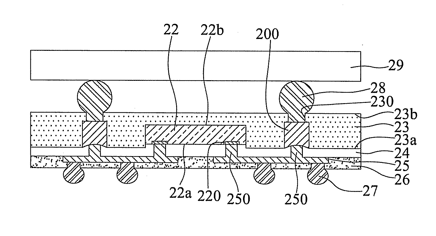
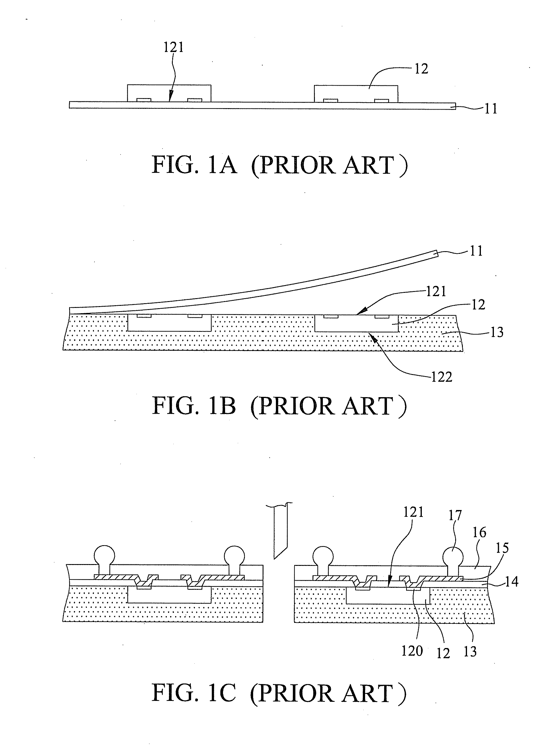
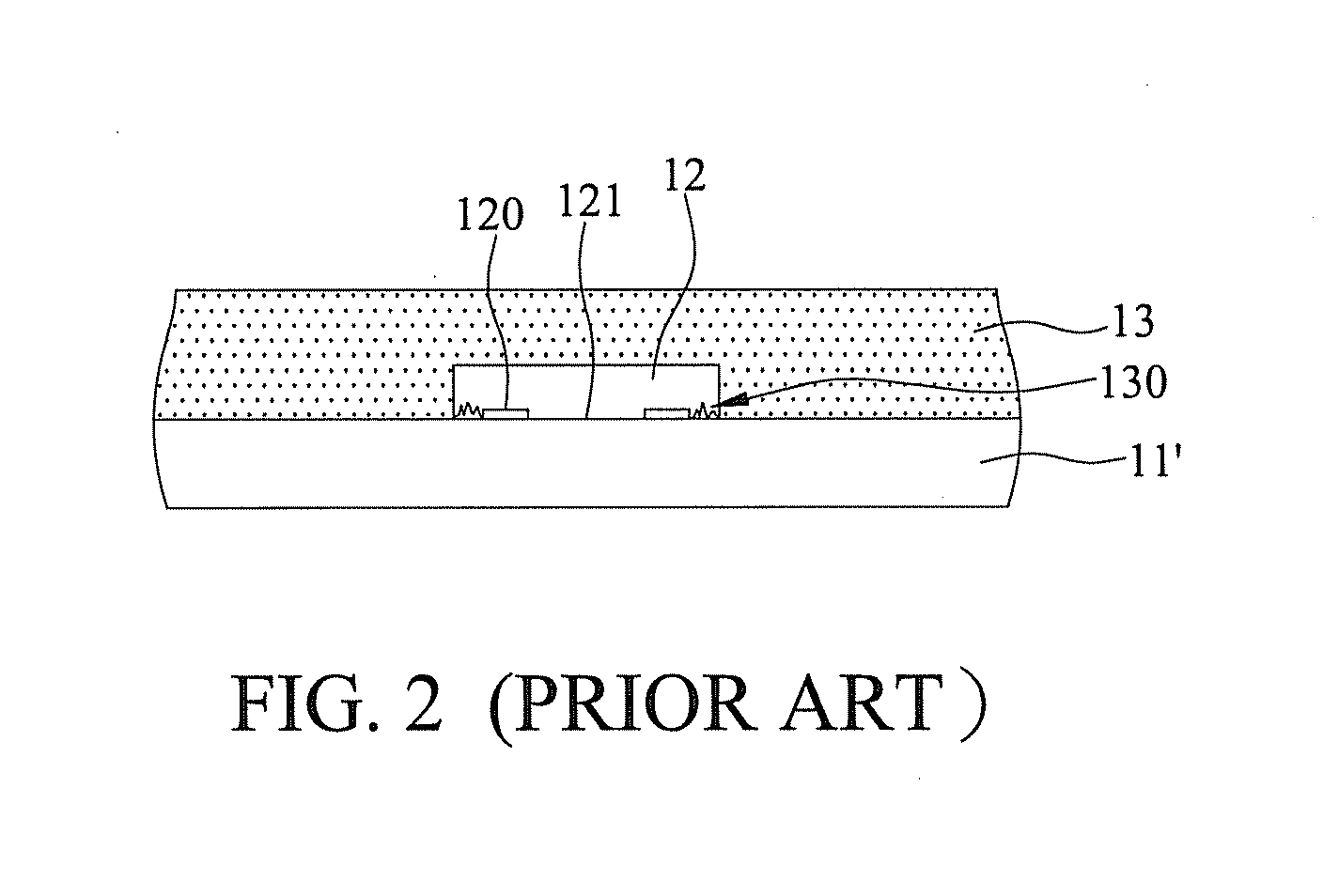
[0046]Likewise, the drawings showing embodiments of the structure are semi-diagrammatic and not to scale and, particularly, some of the dimensions are for the clarity of presentation and are shown greatly exaggerated in the drawings. Similarly, although the views in the drawings for ease of description gener...


PUM


Abstract

A chip scale package and a method of fabricating the chip scale package. The chip scale package includes a encapsulant having a first surface and a second surface opposing the first surface; a conductive pillar formed in the encapsulant and exposed from the first surface and the second surface; a chip embedded in the encapsulant while exposed from the first surface; a dielectric layer formed on the first surface, the conductive pillar and the chip; a circuit layer formed on the dielectric layer; a plurality of conductive blind vias formed in the dielectric layer electrically connecting the circuit layer, electrode pads and the conductive pillar; and a solder mask layer formed on the dielectric layer and the circuit layer, thereby using conductive pillars to externally connect with other electronic devices as required to form a stacked structure.

Description

BACKGROUND OF THE INVENTION[0001]1. Field of the Invention[0002]This invention relates to packages and methods of fabricating the same, and more particularly, to a chip scale package and a method of fabricating the same.[0003]2. Description of Related Art[0004]With the advancement of semiconductor technology, a semiconductor product may be in various package forms. In order to pursue the goal of compact size, a chip scale package (CSP) is brought to the market that is characterized in that the chip scale package is the same as or slightly greater than a chip in size.[0005]U.S. Pat. Nos. 5,892,179, 6,103,552, 6,287,893, 6,350,668 and 6,433,427 disclosed a conventional CSP structure, in which a built-up structure is formed on a chip directly, without using a chip carrier, such as a substrate or a lead frame. A redistribution layer (RDL) technique is used to redistribute electrode pads on the chip to desired locations.[0006]However, the above CSP structure has an disadvantage that the ...

Claims


Application Information

Patent Timeline
IPC IPC(8): H01L23/498H01L21/50
CPCH01L21/561H01L2225/1058H01L23/3114H01L23/3128H01L23/5389H01L24/82H01L2224/04105H01L2224/20H01L2224/82001H01L2924/01029H01L2924/01079H01L2924/01082H01L2924/01033H01L2924/014H01L24/19H01L2225/1035H01L21/568H01L2224/12105H01L2924/18162H01L2224/16235H01L2924/15311
Inventor CHANG, CHIANG-CHENGHUANG, CHIEN-PINGKE, CHUN-CHI
Owner SILICONWARE PRECISION IND CO LTD
Why Eureka
Try Eureka