Device and method for depositing organic material

a technology of organic material and depositing device, which is applied in the direction of liquid surface applicators, semiconductor devices, coatings, etc., can solve the problems of not easy to change the deposition source, abnormal light emission of organic light emitting elements, and non-uniform thickness of organic thin film in the pixel on the substrate, so as to reduce or prevent formation, the thickness of the deposited organic material is substantially uniform, and the effect of improving the uniformity of the deposited organic material

Active Publication Date: 2012-03-15
SAMSUNG DISPLAY CO LTD
View PDF3 Cites 11 Cited by
  • Summary
  • Abstract
  • Description
  • Claims
  • Application Information

AI Technical Summary

Benefits of technology

[0034]According to an embodiment, substantial uniformity of the thickness of the deposited organic material can be achieved (or acquired) by reducing or preventing formation of a shadow effect in the organic material deposition process.
[0035]Also, the uniformity of the thickness of the deposited organic material may be further improved by using an overlapping effect in the organic material deposition process.
[0036]In addition, the flux of the organic material used may be reduced by improving or optimizing the disposition of a nozzle.

Problems solved by technology

Because of the blocking influence by the shield, a shadow effect occurs, resulting in a non-uniform thickness of the organic thin film in the pixel on the substrate.
When the thickness of the organic thin film deposited in the organic light emitting element is not uniformly formed, the organic light emitting element may emit light abnormally and an entire area of the organic light emitting diode (OLED) display may not provide uniform light emission.
It is not easy to change the deposition source in order to reduce or prevent the shadow effect.
Further, when a taper angle of the mask shield is reduced by modifying (or improving) the form of the mask, a gap between openings of the mask may increase and a gap between the pixels may increase, such that a high-resolution organic light emitting diode (OLED) display may not be generated.

Method used


Image

  • Device and method for depositing organic material
  • Device and method for depositing organic material
  • Device and method for depositing organic material

Examples


Embodiment Construction

[0056]The present invention will be described more fully hereinafter with reference to the accompanying drawings, in which exemplary embodiments of the invention are shown.

[0057]The drawings and description are to be regarded as illustrative in nature and not restrictive. Like reference numerals designate like elements throughout the specification. The size and thickness of each component shown in the drawings is arbitrarily shown for understanding and ease of description, but the present invention is not limited thereto.

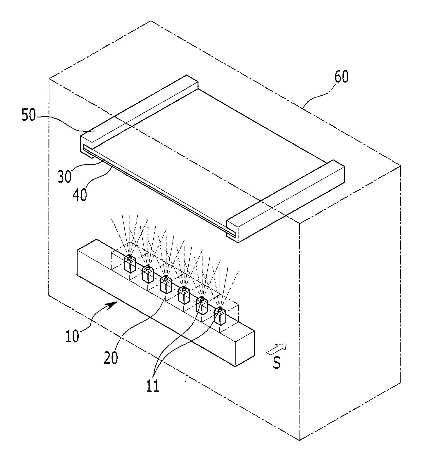
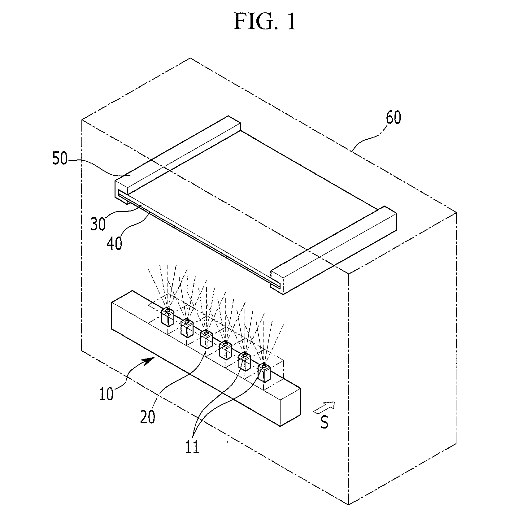
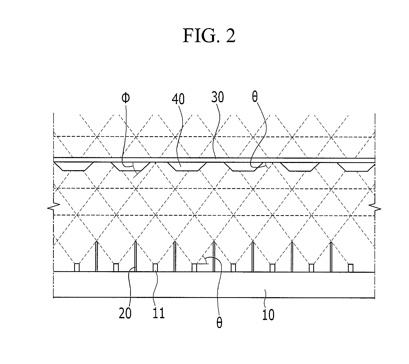
[0058]FIG. 1 shows a perspective view of an organic material depositing device according to a first exemplary embodiment, and FIG. 2 shows a process for depositing an organic material on a substrate using an organic material depositing device according to the first exemplary embodiment. An organic material depositing device according to a present exemplary embodiment will now be described with reference to the drawings.

[0059]Referring to FIG. 1, the organic material...


PUM


Abstract

A device for depositing an organic material includes a substrate; a mask having an opening portion and a shield portion; a fixing member for fixing the substrate and the mask to each other; a deposition source comprising a plurality of nozzles arranged in a first direction and configured to spray the organic material; and a plurality of shield plates near the plurality of nozzles on the deposition source. An angle θ between the substrate and a line extended from a distal end of one of the nozzles to a center of a distal end of a corresponding one of the shield plates is greater than or equal to a taper angle Φ of the shield portion of the mask.

Description

CROSS-REFERENCE TO RELATED APPLICATION[0001]This application claims priority to and the benefit of Korean Patent Application No. 10-2010-0090598 filed in the Korean Intellectual Property Office on Sep. 15, 2010, the entire content of which is incorporated herein by reference.BACKGROUND[0002]1. Field[0003]The described technology relates generally to an organic material depositing device and depositing method.[0004]2. Description of the Related Art[0005]An organic light emitting diode (OLED) display is a flat display device that has a self emissive characteristic and does not require a separate light source, so that it can be made light in weight and thin. An OLED display exhibits quality characteristics such as low power consumption, high luminance, and fast (or high) response speed, and as such, the OLED display receives much attention as a next-generation display device.[0006]In general, an OLED display includes an organic light emitting element that has an anode, an organic emiss...

Claims


Application Information

Patent Timeline
Patent Type & Authority Applications(United States)
IPC IPC(8): H01L21/36B05B15/04
CPCB05B1/14B05B13/04H01L51/0003H01L51/0004H01L51/56B05B15/0443B05B12/36H10K71/13H10K71/00H10K71/12
Inventor CHOI, SEUNG-HOCHOI, HYUNKIM, SUNG-GONSEO, MIN-GYU
Owner SAMSUNG DISPLAY CO LTD
Why Eureka
Try Eureka