

Methods of forming a phase-change material layer pattern, methods of manufacturing a phase-change memory device and related slurry compositions
a technology of phase-change material and layer pattern, which is applied in the direction of solid-state devices, manufacturing tools, lapping machines, etc., can solve the problems of affecting the operation efficiency of the pram device, the damage of the phase-change material layer, and the loss of data stored in the volatile semiconductor memory device. , to achieve the effect of enhancing polishing efficiency, reducing selectivity, and reducing the number o
- Summary
- Abstract
- Description
- Claims
- Application Information
AI Technical Summary
Benefits of technology
Problems solved by technology
Method used
Image

Examples
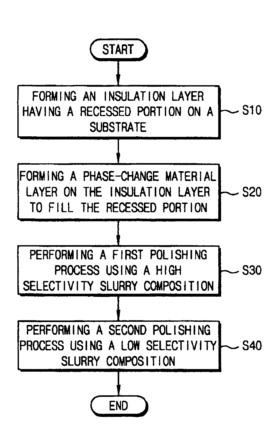
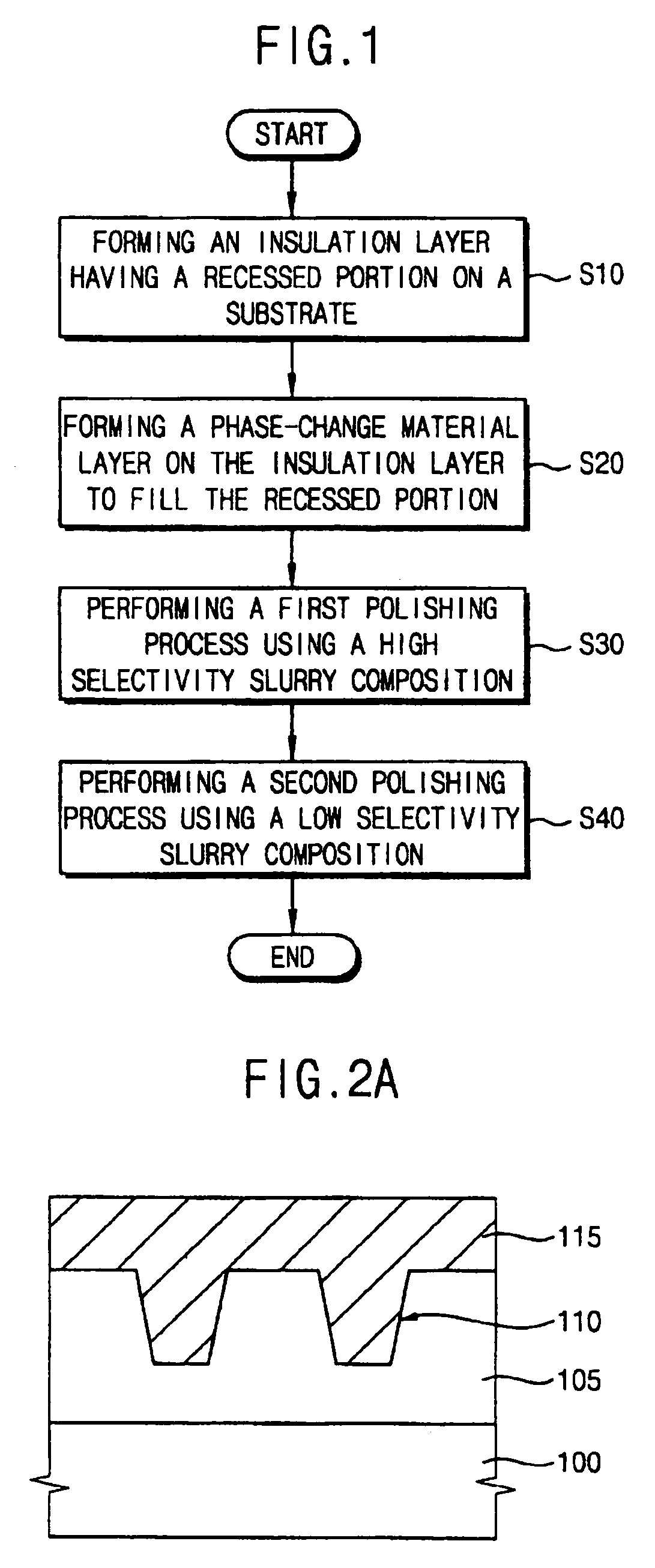
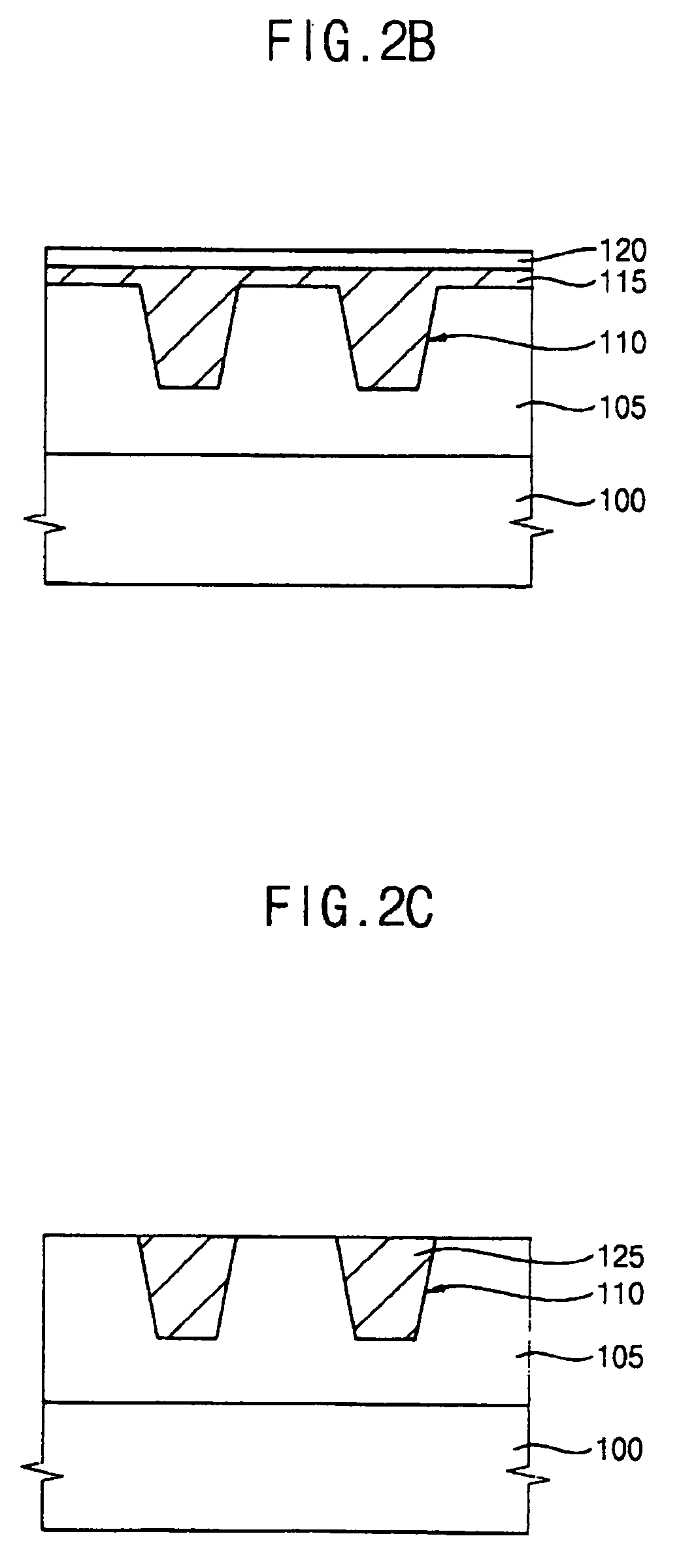
example 1
[0102]A slurry composition was prepared by mixing about 3.5 wt % of colloidal silica, about 3 wt % of citric acid, about 0.2 wt % of hydrogen peroxide, about 0.2 wt % of benzotriazole and a remaining amount of deionized water, and by adding a pH-controlling agent, e.g., hydrochloric acid, to the mixture until the pH of the composition was about 4.0.
examples 2 through 7
[0103]Slurry compositions were prepared by performing a process substantially the same as that of Example 1, except that amounts of the abrasive, citric acid, hydrogen peroxide and benzotriazole were changed. The amounts of the abrasive, citric acid, hydrogen peroxide and benzotriazole are shown in Table 1. The unit of the amount is percent by weight.
[0104]
TABLE 1SilicaCitric AcidHydrogen PeroxideBenzotriazoleExample 13.530.20.2Example 23.530.1—Example 33.530.2—Example 410.50.2—Example 510.50.20.1Example 610.50.20.2Example 710.50.20.3
[0105]Evaluation of Polishing Rates and Polishing Selectivity
[0106]A polishing process was performed on a phase-change material layer and a silicon oxide layer using each of the slurry compositions prepared in Examples 1 through 7 to evaluate polishing selectivities of the slurry compositions.
[0107]The phase-change material layer was formed on a silicon wafer by performing a CVD process using germanium-antimony-tellurium (GST). The phase-change material...
PUM
| Property | Measurement | Unit |
|---|---|---|
| mean diameter | aaaaa | aaaaa |
| mean diameter | aaaaa | aaaaa |
| flow rate | aaaaa | aaaaa |
Abstract
Description
Claims
Application Information