Systems and methods for averaging error rates in non-volatile devices and storage systems

a non-volatile device and error rate technology, applied in error prevention, digital transmission, instruments, etc., can solve problems such as deterioration of original physical level into current charge level, and achieve the effects of reducing probability, high probability, and improving programming speed

Active Publication Date: 2012-03-15
AVAGO TECH INT SALES PTE LTD
View PDF5 Cites 190 Cited by
  • Summary
  • Abstract
  • Description
  • Claims
  • Application Information

AI Technical Summary

Benefits of technology

[0015]The following terms may be construed either in accordance with any definition thereof appearing in the prior art literature, or in accordance with any definition implied by any portion of the specification, or as follows: Bank, flash memory bank=ordered set (e.g. sequence or array) of flash memory), all connected to a single data source, such as a PC through the USB interface sr, via a unique and separate interface such as NAND Flash interface. Since different banks each may be connected to the data source via their own interface, they may be accessible in parallel. Bit error rate=the average proportion of bits within a physical page, which are erroneous. This may be measured through experiments in which several pages (of the same type) are programmed and following cycling and retention are read back and compared to their original contents. The bit error rate is then the ratio between the average number of bit errors per page and the length of the page in bits. The bit error rate (BER) may vary between individual devices. Block=a set of flash memory device cells which must, due to physical limitations of the flash memory device, be erased together. Also termed erase sector, erase block. Each block typically comprises an ordered set (e.g. sequence or array) of at least one physical page which are all erased simultaneously by each erase operation, the set typically comprising a predetermined number of typically physically adjacent physical pages. Cell: Apparatus into which any of at least two statistically distinguishable ranges of a physical quantity, such as electrical charge, can be induced. Each detectably distinct range has a predetermined association with a digital value, also termed herein “logical value”, which is said to be “stored” in the cell. Since induction in a cell, of a target amount of a physical quantity is typically not deterministic and instead typically modeled by a random, Gaussian process centered about the target amount, “storing” an individual digital value in a cell typically comprises striving to induce, in that cell, a target amount of the physical quantity which comprises the center of the range pre-associated with the individual digital value. As a result, the actual amount induced in the cell is, statistically, almost always within the range associated with the individual digital value, at least initially, hence the individual digital value can, statistically, almost always be correctly read from the cell, at least initially. In flash memory applications, a component of flash memory that stores one bit of information (in single-level cell devices) or n bits of information (in a multi-level device having 2 exp n levels). Typically, each cell comprises a floating-gate transistor. n may or may not be an integer. Charge level or degraded level: Amount of charge currently existing in a cell, as opposed to “program level”, the amount of charge originally induced in the cell which typically exceeds the current (charge) level due to the phenomenon of gradual degradation of the amount of charge in a cell, over time. Cycling: Repeatedly writing new data into flash memory cells and repeatedly erasing the cells between each two writing operations. Demapping: basic cell-level reading function in which incoming digital n-type data is derived from a physical value representing a physical state in the cell having a predetermined correspondence to the incoming digital value. Digital value: n-tuple of bits represented by a cell in flash memory capable of generating 2 exp n distinguishable levels of a physical value such as charge, where n may or may not be an integer. Erase cycle: The relatively slow process of erasing a block of cells, or, in certain non-flash memory devices, of erasing a single cell or the duration of so doing. An advantage of erasing cells collectively in blocks as in flash memory, rather than individually, is enhanced programming speed: Many cells are erased in a single erase cycle. Erase-write cycle: The process of erasing a block of cells and subsequently writing new data into at least some of them. Flash memory: Non-volatile rewritable computer memory including cells that are erased in blocks rather than individually, but are written into and read from, in smaller units e.g. individually or page by page where at least some of the blocks include more than one page each. Includes NOR-type flash memory, NAND-type flash memory, and PRAM, e.g. Samsung PRAM, inter alia. A flash memory device typically comprises ordered set (e.g. sequence or array) of flash memory cells in conjunction with reading circuitry, writing circuitry and erasing circuitry. Input / output sequence=I / O sequence=transaction: Request from host to read or write a given number of logical pages from or to a flash memory system. A sequence is “short” if the number of logical pages is less than the number of banks in the flash memory system. Interleaving: When writing a logical page into flash memory, distributing the data therein over disparate locations in the flash memory, so as to greatly diminish the probability that the logical page will be stored at a poor quality portion of the flash memory, such that the logical page, when read, will contain more errors than its error correction code can overcome. Distribution need not be regular or strictly alternating. Mapping: basic cell-level writing function in which incoming digital n-tuple is mapped to a physical value by inducing a physical state in the cell, having a predetermined correspondence to the incoming digital value. Page=A portion, typically 512 or 2048 or 4096 bytes in size, of a memory device such as a NAND flash memory device Writing can be performed page by page, as opposed to erasing which can be performed only erase sector by erase sector. A few bytes, typically 16-32 for every 512 data bytes (termed redundancy bytes) are associated with each page (typically 16, 64 or 128 per page), for storage of error correction information. A typical block may include 32 512-byte pages or 64 2048-byte pages. Precise read, soft read: Read the cell threshold voltage in precision greater than the number of the Mapping levels (2 n). The terms precise read or soft read are interchangeable. Programming: The process of writing new data in at least some of the pages of an erase sector. Program level (or: programmed level, originally written level): amount of charge originally induced in a cell to represent a given digital value, as opposed to “charge level”. Reprogrammability (Np): An aspect of flash memory quality. This is typically operationalized by a reprogrammability parameter, also termed herein “Np”, denoting the number of times that a flash memory or a sub-section of the memory such as a page can be re-programmed (number of erase-write cycles that the device can withstand) before the level of errors is so high as to make an unacceptably number of those errors irrecoverable with high probability given a predetermined amount of memory devoted to redundancy. Typically recoverability is investigated following a conventional aging simulation process which simulates or approximates the data degradation effect that a predetermined time period e.g. a 10 year period has on the flash memory device, in an attempt to accommodate for a period of up to 10 years between writing of data in flash memory and reading of the data therefrom. Retention: of original physical levels induced in the cells; retention is typically below 100% resulting in deterioration of original physical levels into current charge levels. Retention time: Flash storage time without voltage supply or specifically the elapse time between page programs to page read. Symbol: Digital value Logical page: a portion of typically sequential data, whose amount is typically less than or equal to a predetermined amount of data defined to be a pageful of data, which has typically been defined by a host (data source / destination) or user thereof, as a page, and which is sent by the host to a flash memory device for storage and is subsequently read by the host from the flash memory device. Physical page: ordered set (e.g. sequence or array) of flash memory cells which are all written in simultaneously by each write operation, the set typically comprising a predetermined number of typically physically adjacent flash memory cells containing actual data written by and subsequently read by the host, as well as, typically error correction information and back pointers used for recognizing the true address of a page. Pagelet: portion of a logical page which is to be written onto a particular physical page. Reliability: Reliability of a flash memory device may be operationalized as the probability that a worst-case logical page written and stored in that device for a predetermined long time period such as 10 years will be successfully read i.e. that sufficiently few errors, if any, will be present in the physical page / s storing each logical page such that the error code appended to the logical page will suffice to overcome those few errors.

Problems solved by technology

Retention: of original physical levels induced in the cells; retention is typically below 100% resulting in deterioration of original physical levels into current charge levels.

Method used


Image

  • Systems and methods for averaging error rates in non-volatile devices and storage systems
  • Systems and methods for averaging error rates in non-volatile devices and storage systems
  • Systems and methods for averaging error rates in non-volatile devices and storage systems

Examples


Embodiment Construction

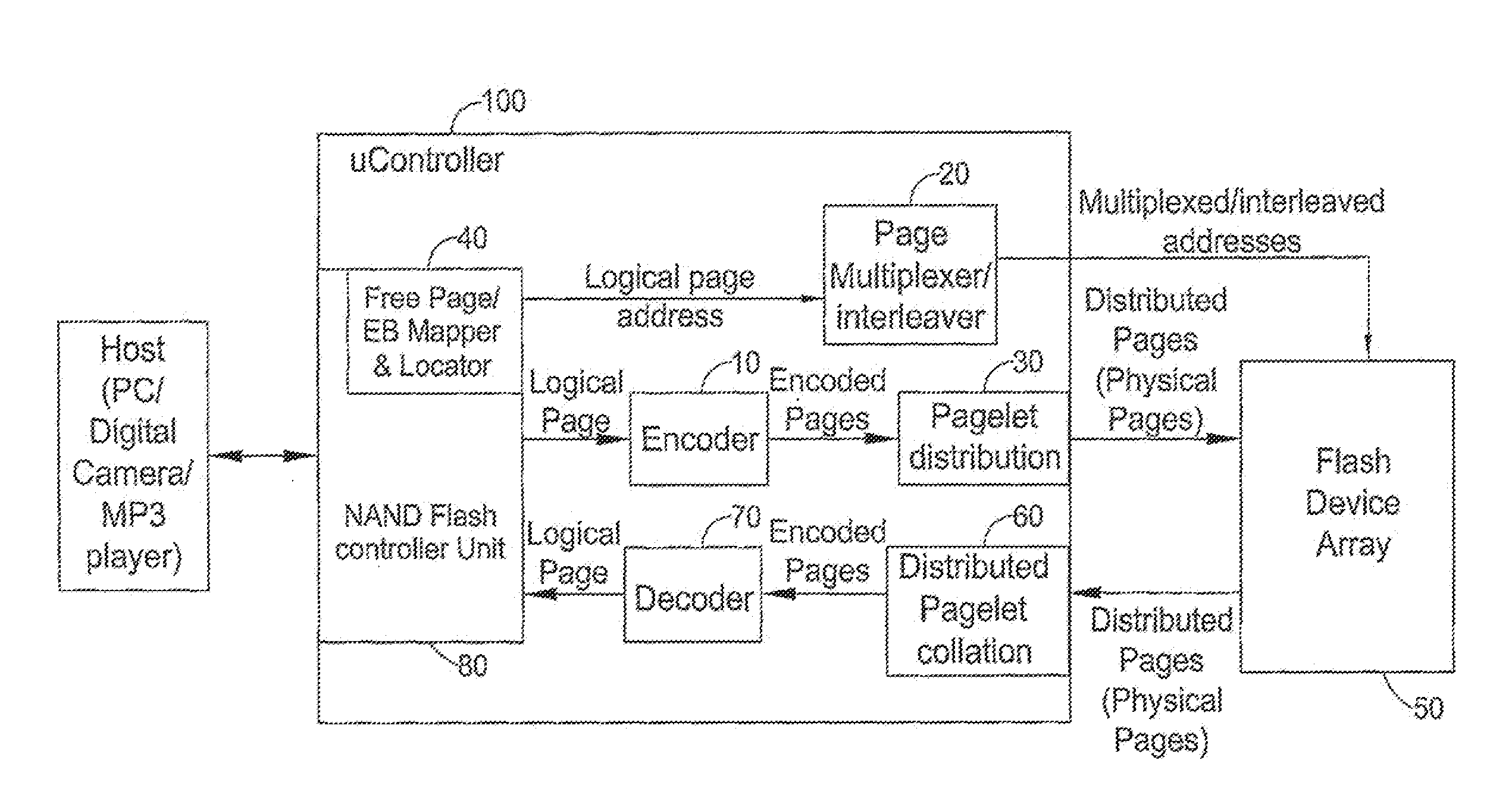
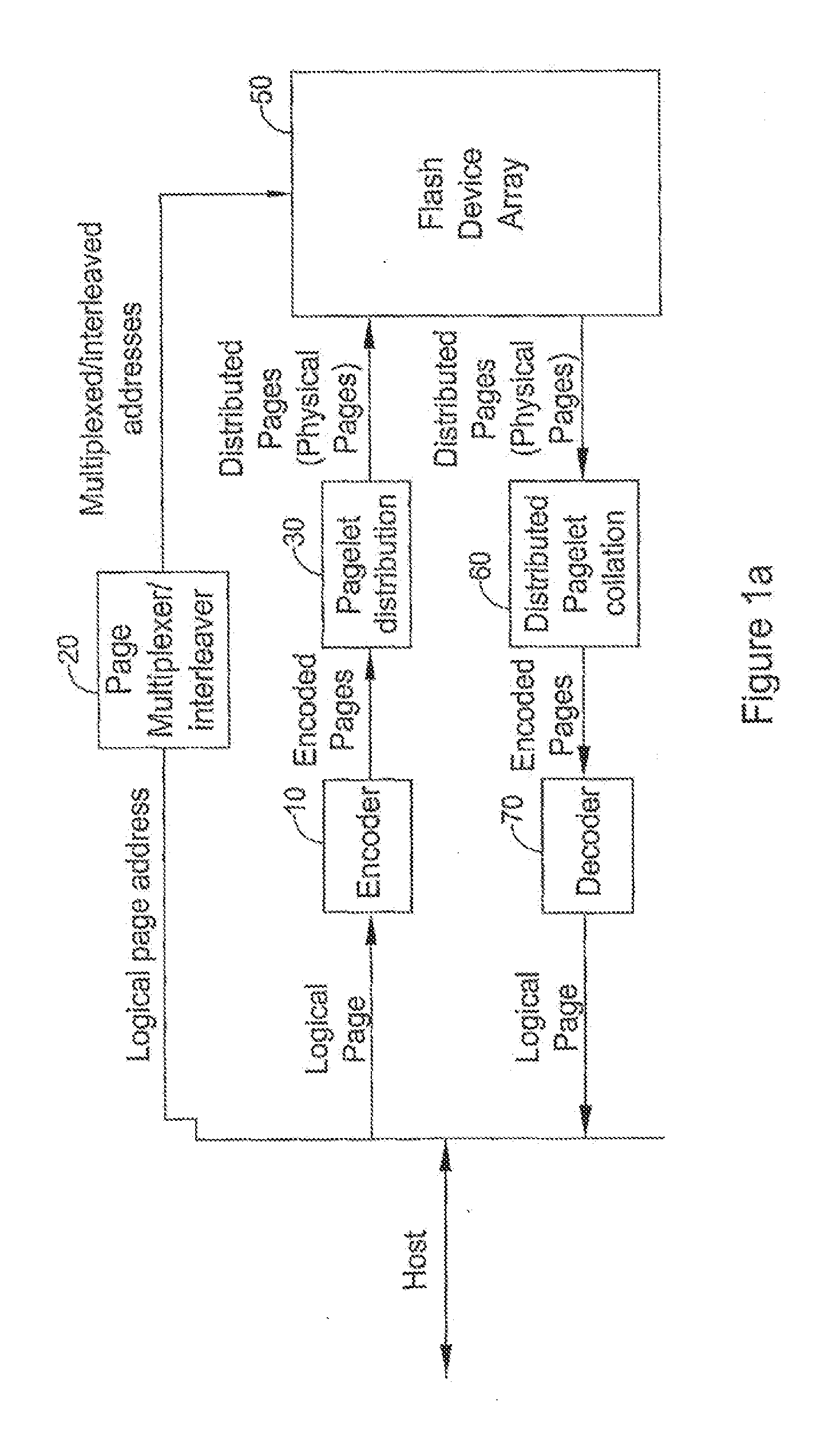
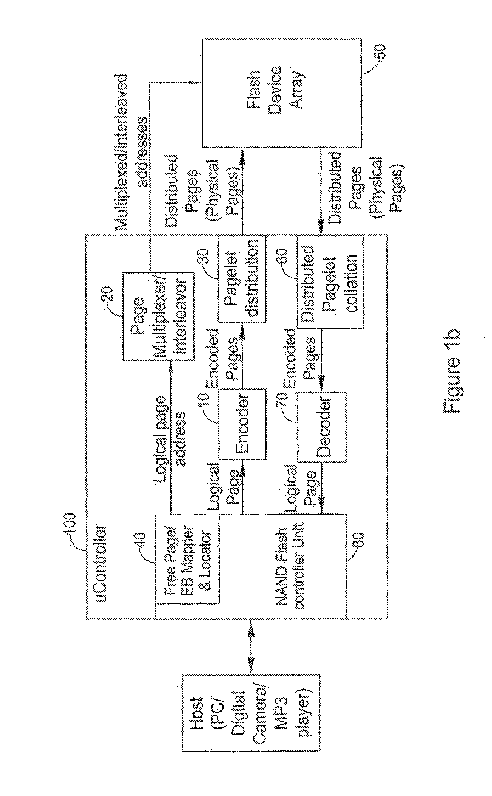
[0065]Today's Flash memory devices store information as charge in either a floating gate transistor or an NROM transistor. Multi-Level Cells (MLC) store several bits by setting the amount of charge in the cell. The amount of charge is then measured by a detector, e.g. by a threshold voltage of the cell's transistor gate. Due to inaccuracies during the multiple erase and programming procedures and because of charge loss due to time and temperature (also known as retention), the measured levels suffer from a random distortion. As a result, some errors appear when the device is read. This reliability is then measured by the error probability or by a bit error rate (BER).

[0066]Flash devices are organized into pages. Each page contains a section allocated for data (512 bytes-4 Kbytes) and a small amount of bytes (16-32 bytes for every 512 data bytes) allocated for redundancy and back pointers. The redundancy bytes are used to store error correcting information, for correcting errors whic...


PUM


Abstract

A system for storing a plurality of logical pages in a set of at least one flash device, each flash device including a set of at least one erase block, the system comprising apparatus for distributing at least one of the plurality of logical pages over substantially all of the erase blocks in substantially all of the flash devices, thereby to define, for at least one logical page, a sequence of pagelets thereof together including all information on the logical page and each being stored within a different erase block in the set of erase blocks; and apparatus for reading each individual page from among the plurality of logical pages including apparatus for calling and ordering the sequence of pagelets from different erase blocks in the set of erase blocks.

Description

REFERENCE TO CO-PENDING APPLICATIONS[0001]This application is a DIVISIONAL of, claims priority to and incorporates by reference U.S. patent application Ser. No. 12 / 595,964, filed Oct. 15, 2009, which is a NONPROVISIONAL of, claims priority to and incorporates by reference U.S. Provisional Application No. 60 / 960,943, filed Oct. 22, 2007 and entitled “Systems and methods to reduce errors in Solid State Disks and Large Flash Devices” and U.S. Provisional Application No. 61 / 071,469, filed Apr. 30, 2008 and entitled “Systems and Methods for Averaging Error Rates in Non-Volatile Devices and Storage Systems”.[0002]Other co-pending applications include: U.S. Provisional Application No. 60 / 960,207, filed Sep. 20, 2007 and entitled “Systems and Methods for Coupling Detection in Flash Memory”, U.S. Provisional Application No. 61 / 071,467, filed Apr. 30, 2008 and entitled “Improved Systems and Methods for Determining Logical Values of Coupled Flash Memory Cells”, U.S. Provisional Application No....

Claims


Application Information

Patent Timeline
Patent Type & Authority Applications(United States)
IPC IPC(8): G06F12/00
CPCG06F11/1068G06F12/0246G06F2212/1032H04L1/203G06F2212/7208G11C16/0483G06F2212/7202
Inventor WEINGARTEN, HANAN
Owner AVAGO TECH INT SALES PTE LTD
Why Eureka
Try Eureka