Phototransistor and display device including the same

a technology of phototransistor and display device, which is applied in the direction of transistors, optics, instruments, etc., can solve the problems of reduced sensor sensitivity and increased thickness of display device, and achieve the effect of reducing accumulated charge and maintaining favorable light-receiving characteristics of phototransistor

Inactive Publication Date: 2012-03-29
SHARP KK
View PDF1 Cites 12 Cited by
  • Summary
  • Abstract
  • Description
  • Claims
  • Application Information

AI Technical Summary

Benefits of technology

[0026]According to the present invention, a voltage is applied between a transparent electrode, and a gate electrode and a source electrode by a refresh controller, thereby reducing a charge accumulated in a portion of a channel region, the portion facing a transparent electrode. Thus, light-receiving characteristics of the phototransistor can be favorably maintained.

Problems solved by technology

However, the problem in this technique was that the thickness of the display device was increased.
However, characteristics of the optical sensors, such as phototransistors, may deteriorate with time and use, which may result in a reduction in sensitivity of the sensors.

Method used


Image

  • Phototransistor and display device including the same
  • Phototransistor and display device including the same
  • Phototransistor and display device including the same

Examples


embodiment of invention

[0035]FIGS. 1-7 show an embodiment of the present invention.

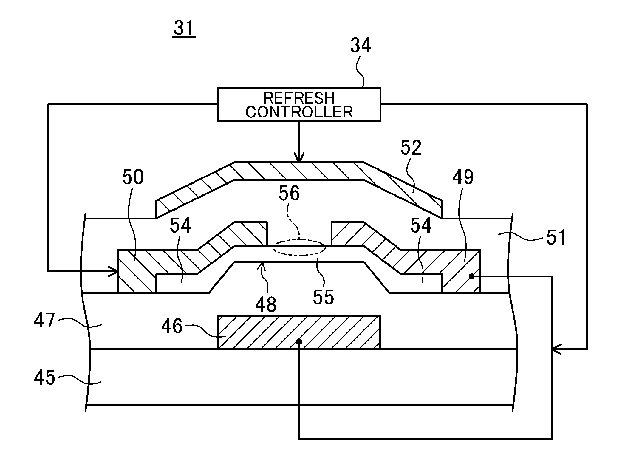
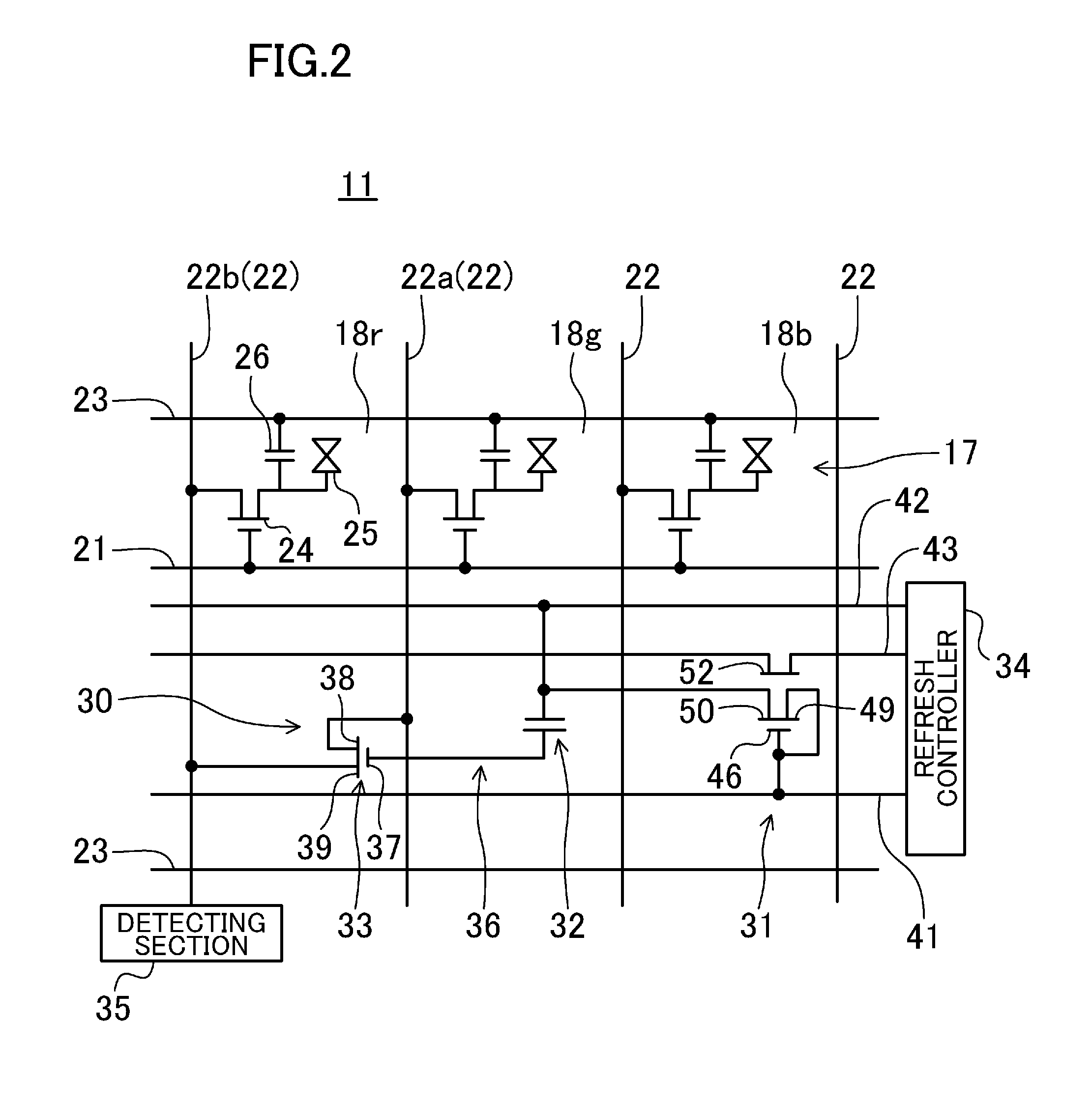
[0036]FIG. 1 is an enlarged cross-sectional view of a structure of a phototransistor 31 in the present embodiment. FIG. 2 is a circuit diagram showing pixels 17 of a liquid crystal display device 1 in the present embodiment. FIG. 3 is a timing chart for explaining an operation of a touch location detector 30. FIG. 4 is a flowchart showing an operation of the phototransistor 31 in the present embodiment. FIG. 5 is a cross-sectional view schematically showing a structure of the liquid crystal display device 1 of the present embodiment.

[0037]In the present embodiment, the liquid crystal display device 1 will be described as an example display device.

[0038]—Structure of Liquid Crystal Display Device—

[0039]The liquid crystal display device 1 includes a liquid crystal display panel 10 and a backlight unit 15 located on the back side of the liquid crystal display panel 10 (i.e., on the side opposite to the side facing the user) as...

first embodiment

Effect of First Embodiment

[0080]According to this first embodiment, the phototransistor 31 is provided with the transparent electrode 52 and the refresh controller 34. A voltage is applied between the transparent electrode 52, and the gate electrode 46 and the source electrode 49, by the refresh controller 34, thereby making it possible to form an electric field in the back channel 56. The charge accumulated in the back channel 56 due to continuous light receiving can be reduced by this electric field. As a result, carriers in the channel region 55 can move easily, and the light-receiving characteristics of the phototransistor 31 can be brought close to the initial state. Thus, generating the electric field (i.e., performing refresh control) by this refresh controller 34 at every predetermined time can maintain favorable light-receiving characteristics of the phototransistor 31, and high sensor accuracy.

[0081]Further, the refresh control by the refresh controller 34 is performed at ...


PUM


Abstract

A phototransistor includes a source electrode and a gate electrode which have the same electric potential, a transparent electrode formed on a surface of an interlayer insulating film so as to be located above a channel region, and a refresh controller for reducing a charge accumulated in a portion of the channel region, the portion facing the transparent electrode, by applying a voltage between the transparent electrode, and the gate electrode and the source electrode.

Description

TECHNICAL FIELD[0001]The present invention relates to a phototransistor and a display device including the phototransistor.BACKGROUND ART[0002]In recent years, attention has been given to touch panel devices as input means for devices. A resistive layer type, an optical type, etc., are generally known as types of the touch panel devices. For example, layering the touch panel devices on a liquid crystal display panel to provide a liquid crystal display device with a touch panel had been known. However, the problem in this technique was that the thickness of the display device was increased. To reduce the thickness of the device as a whole, providing a plurality of optical sensors to the liquid crystal display panel so that the liquid crystal display panel itself has a function of a touch panel has been known. The optical sensors are, for example, phototransistors.[0003]In the liquid crystal display panel which has a function of a touch panel, a current flows in the optical sensors in...

Claims


Application Information

Patent Timeline
Patent Type & Authority Applications(United States)
IPC IPC(8): H01L31/0224
CPCG02F2001/13312H01L27/14612H01L27/14643H01L27/14678G06F3/0421H01L27/14692H01L31/1136G06F3/0412H01L27/14681G02F1/13312
Inventor KITAGAWA, HIDEKIIMAI, HAJIMEMURAI, ATSUHITO
Owner SHARP KK
Why Eureka
Try Eureka