Circuit board for signal transmission and method of manufacturing the same

a technology of circuit boards and signal transmission, applied in the direction of printed circuits, non-metallic protective coating applications, conductive pattern formation, etc., can solve the problem of increasing noise affected by external environments, and achieve the effect of reducing nois

Inactive Publication Date: 2012-04-05
SAMSUNG ELECTRO MECHANICS CO LTD
View PDF4 Cites 13 Cited by
  • Summary
  • Abstract
  • Description
  • Claims
  • Application Information

AI Technical Summary

Benefits of technology

[0007]The present invention has been invented in order to overcome the above-described problems and it is, therefore, an object of the present invention to provide a cir

Problems solved by technology

However, since the serial interface has a high transmission speed of each channel, if

Method used


Image

  • Circuit board for signal transmission and method of manufacturing the same
  • Circuit board for signal transmission and method of manufacturing the same
  • Circuit board for signal transmission and method of manufacturing the same

Examples


first embodiment

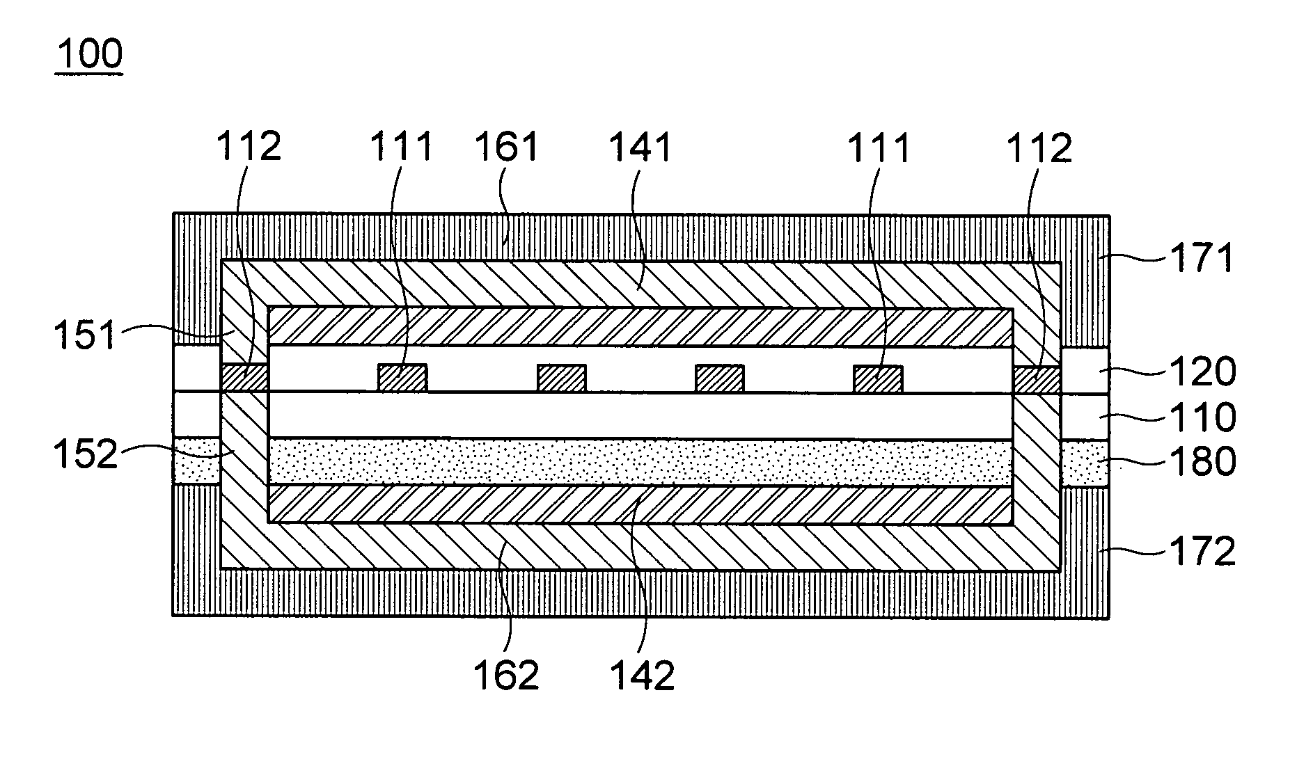
[0052]Therefore, as described in the present invention, since the shield members are provided to surround the plurality of signal interconnections, the noises and electromagnetic waves from the exterior can be blocked and interference with the external signal line can also be securely blocked.

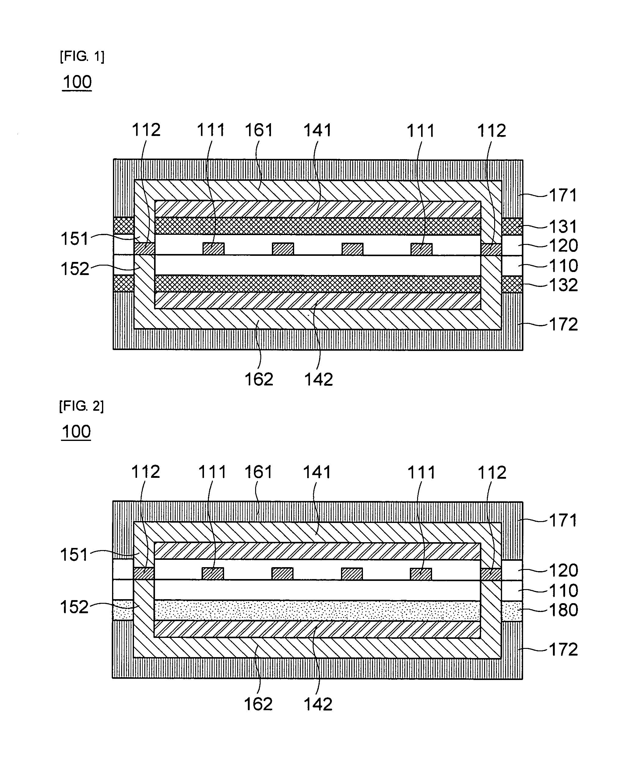
[0053]FIG. 2 is a cross-sectional view of a circuit board for signal transmission in accordance with a second exemplary embodiment of the present invention. Here, except that the insulating layer is further provided instead of the adhesion layer, the circuit board for signal transmission in accordance with a second exemplary embodiment of the present invention may have the same constitution as the circuit board for signal transmission in accordance with a first exemplary embodiment of the present invention. Accordingly, the same description of the second embodiment as the first embodiment will not be repeated, and like elements are designated by like reference numerals.

[0054]Referring to FIG. 2...

third embodiment

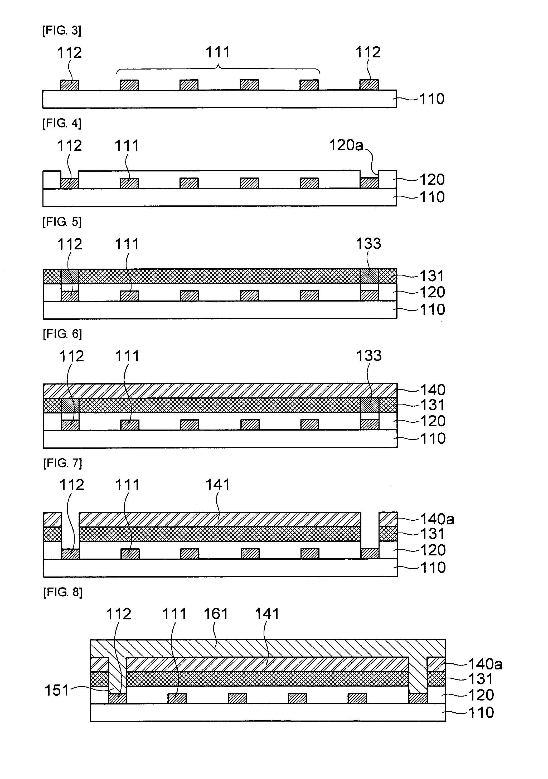
[0087]Here, a process of manufacturing a circuit board for signal transmission in accordance with a fourth exemplary embodiment of the present invention is the same as the process of manufacturing a circuit board for signal transmission of the third embodiment, except that the release layer is not formed, and detailed description thereof will not be repeated.

[0088]Referring to FIG. 13, in order to manufacture the circuit board for signal transmission in accordance with a fourth exemplary embodiment of the present invention, a plurality of signal interconnections 111 and ground interconnections 112 disposed at both sides of the plurality of signal interconnections 111 are formed on a first insulating layer 110.

[0089]Next, a second insulating layer 120, a first adhesion layer 131 and a first metal layer 140 are sequentially formed on the first insulating layer 110 including the plurality of signal interconnections 111 and ground interconnections 112. Here, the second insulating layer ...

fourth embodiment

[0099]Here, a process of manufacturing a circuit board for signal transmission in accordance with a fifth exemplary embodiment of the present invention may include the same manufacturing process as the fourth embodiment, except that the adhesion layer is not formed, and detailed description thereof will not be repeated.

[0100]Referring to FIG. 16, in order to manufacture a circuit board for signal transmission in accordance with a fifth exemplary embodiment of the present invention, first, a plurality of signal interconnection 111 and ground interconnections 112 disposed at both sides of the plurality of signal interconnections 111 are formed on a first insulating layer 110.

[0101]A second insulating layer 120 including a metal layer is provided on the first insulating layer 110 including the plurality of signal interconnections 111 and ground interconnections 112. Here, the second insulating layer 120 including the metal layer may be formed of a resin coated copper (RCC).

[0102]Referr...


PUM

PropertyMeasurementUnit
Adhesion strengthaaaaaaaaaa
aaaaaaaaaa

Abstract

Provided is a circuit board for signal transmission and a method of manufacturing the same. The circuit board for signal transmission includes a first insulating layer, a plurality of signal interconnection disposed on the first insulating layer, ground interconnections disposed on the first insulating layer at both sides of the plurality of signal interconnections, a second insulating layer disposed on the first insulating layer including the plurality of signal interconnections and ground interconnections, a first shield layer disposed on the second insulating layer, a first shield wall for electrically connecting the ground interconnections and the first shield layer and passing through the second insulating layer, a second shield layer disposed under the first insulating layer, and a second shield wall for electrically connecting the ground interconnections and the second shield layer and passing through the first insulating layer.

Description

[0001]This application claims the benefit under 35 U.S.C. Section 119 of Korean Patent Application Serial No. 10-2010-0096604, entitled CIRCUIT BOARD FOR SIGNAL TRANSMISSION AND METHOD OF MANUFACTURING THE SAME filed on Oct. 5, 2010, which is hereby incorporated by reference in its entirety into this application.BACKGROUND OF THE INVENTION[0002]1. Field of the Invention[0003]The present invention relates to a circuit board for signal transmission and a method of manufacturing the same, and more particularly, to a circuit board for signal transmission capable of reducing noises, and a method of manufacturing the same.[0004]2. Description of the Related Art[0005]In recent times, as displays evolve as high resolution displays such as Full HDTV and 3D TV, a large capacity of signal transmission between a display drive circuit and a T-Con board is needed. Accordingly, an image transmission cable is converted from a parallel interface of a low-voltage differential signaling type into a se...

Claims


Application Information

Patent Timeline
IPC IPC(8): H05K9/00H05K3/02H05K3/46
CPCH05K1/0221H05K3/28Y10T29/49155Y10T29/49156H05K2201/0195
Inventor YOO, JE GWANGCHOI, BONG KYUAN, YONG SOO
Owner SAMSUNG ELECTRO MECHANICS CO LTD
Why Eureka
Try Eureka