Wireless IC device and coupling method for power feeding circuit and radiation plate
- Summary
- Abstract
- Description
- Claims
- Application Information
AI Technical Summary
Benefits of technology
Problems solved by technology
Method used
Image
Examples
first preferred embodiment
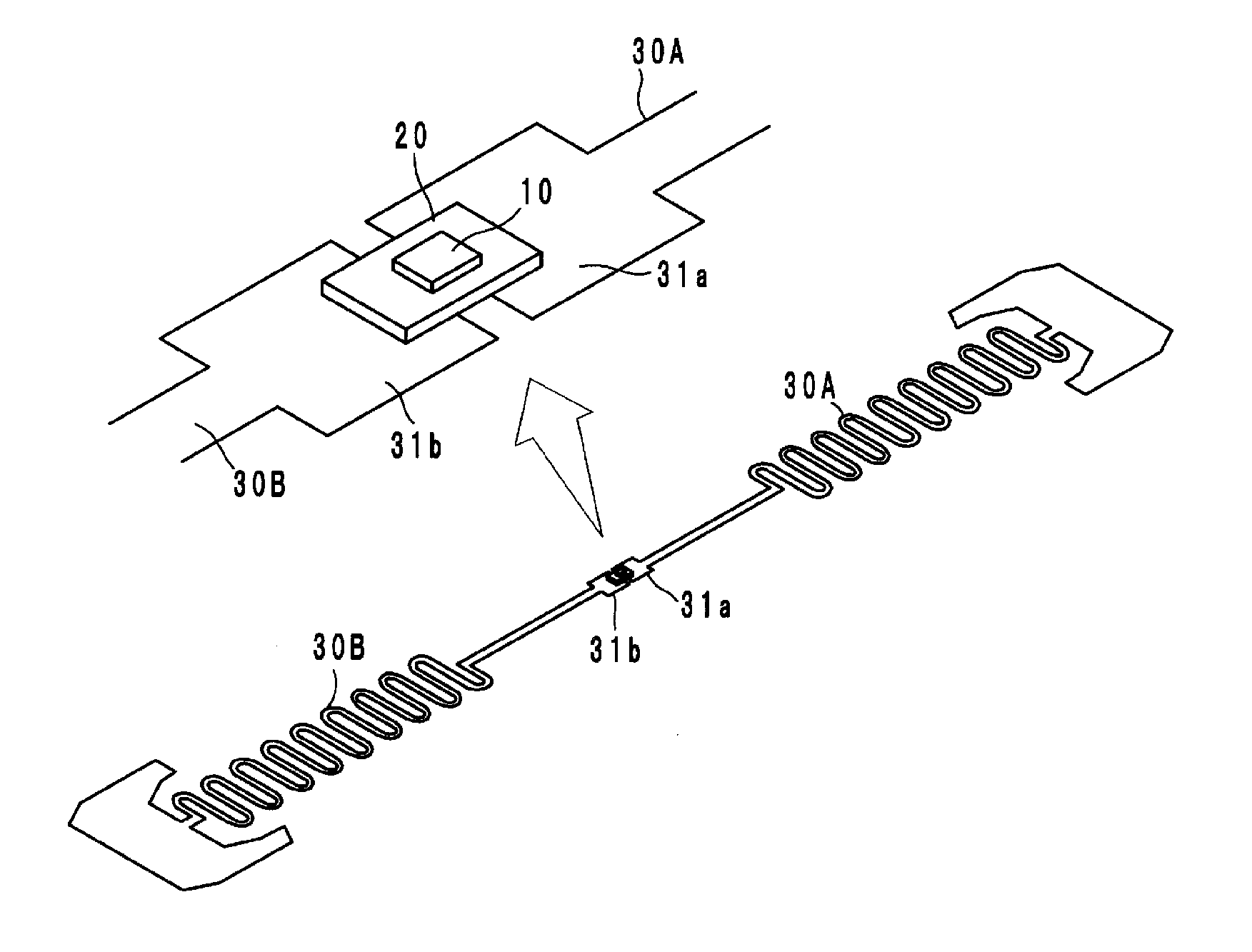
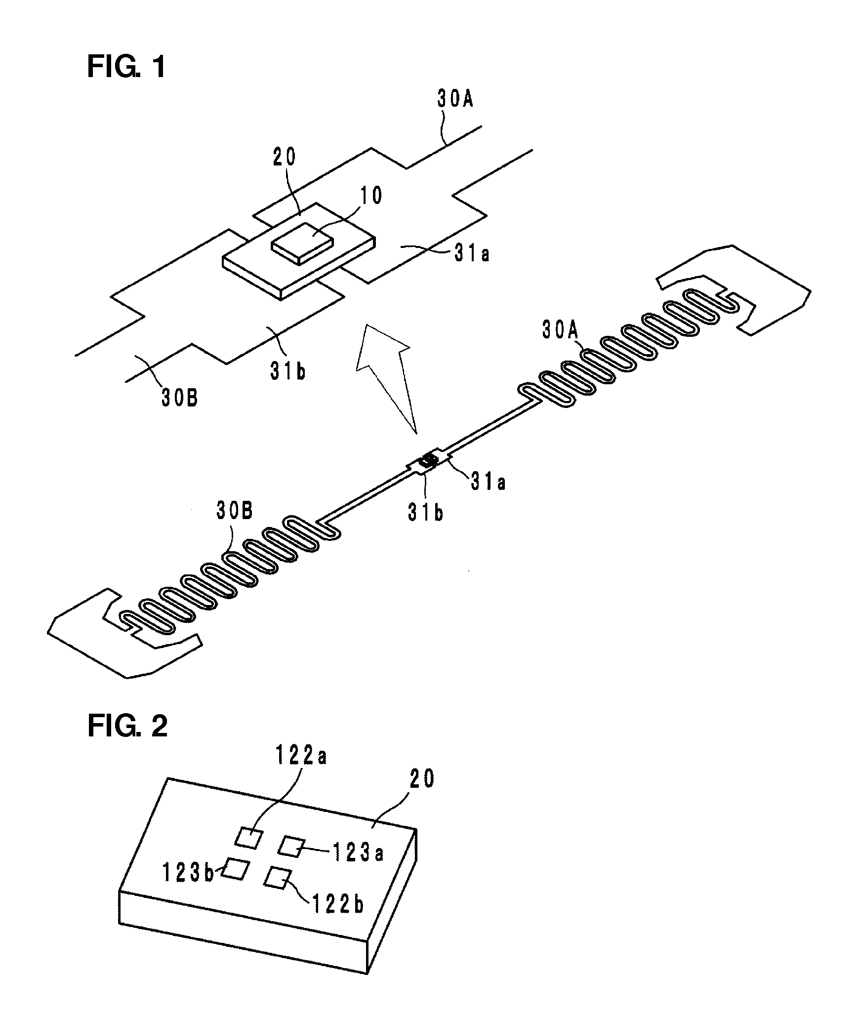
[0034]A wireless IC device that is a first preferred embodiment is a device used in a UHF band, and, as illustrated in FIG. 1, includes a wireless IC chip 10 processing a transmission / reception signal of a predetermined frequency, a power feeding circuit substrate 20 mounted with the wireless IC chip 10, and two radiation plates 30A and 30B.
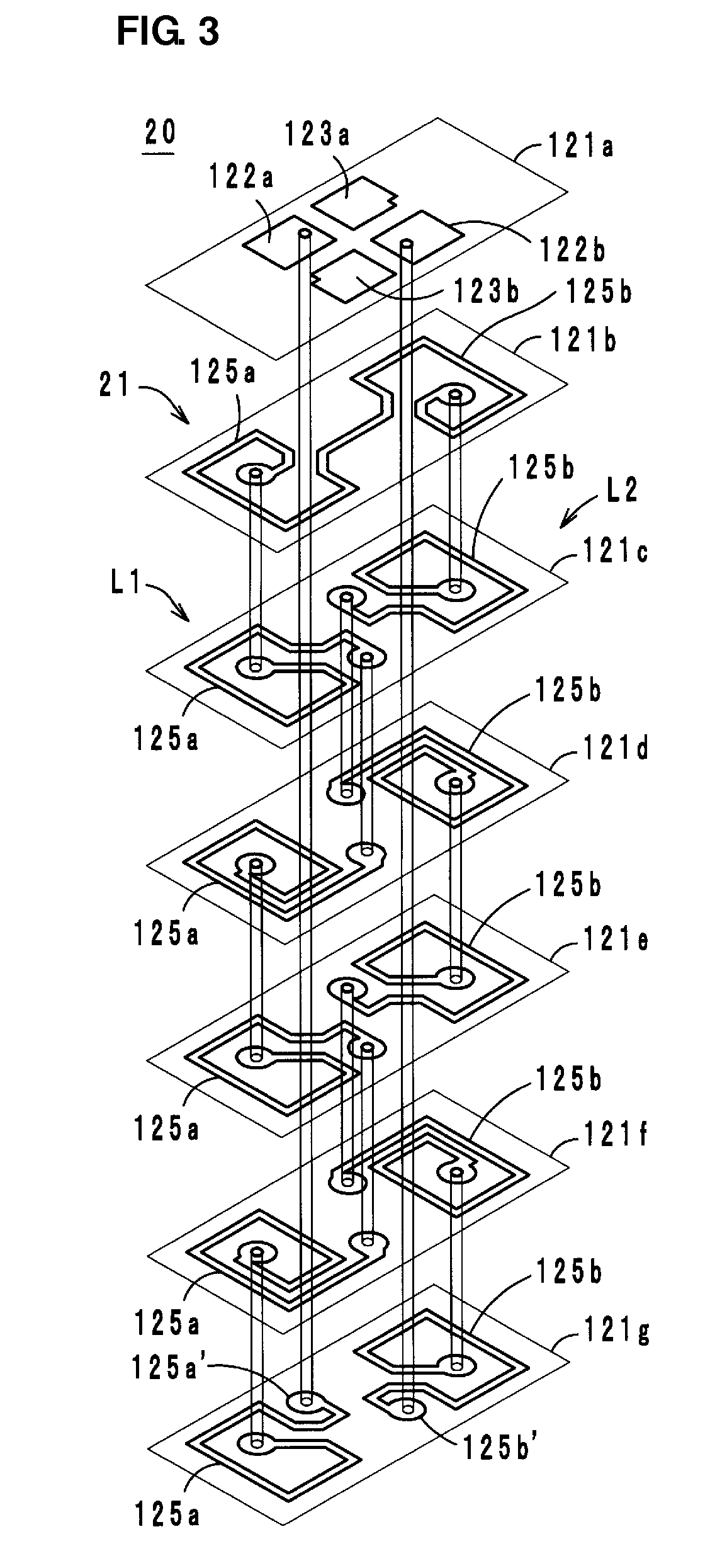
[0035]As illustrated as an equivalent circuit in FIG. 4, the power feeding circuit substrate 20 includes a power feeding circuit 21 including a resonant circuit / matching circuit in which inductance elements L1 and L2 are included that have substantially the same inductance values and preferably have spiral shapes wound in directions opposite to each other. The winding axes of the inductance elements L1 and L2 are disposed at different positions and parallel or substantially parallel to each other, in plan view.
[0036]The wireless IC chip 10 includes a clock circuit, a logic circuit, a memory circuit, and the like, necessary information is stored t...
second preferred embodiment
[0050]As illustrated in FIG. 8, in a wireless IC device according to a second preferred embodiment of the present invention, a radiation plate 30 including the plate-shaped coupling units 31a and 31b is loop-shaped, and the other components are preferably the same as those of the first preferred embodiment. The plate-shaped coupling units 31a and 31b are perpendicularly or substantially perpendicularly disposed in a vicinity of the inductance elements L1 and L2 wound in directions opposite to each other, and hence the power feeding circuit 21 is coupled with the plate-shaped coupling units 31a and 31b owing to eddy currents, and a current flows through the loop-shaped radiation plate 30. This is the same as described in the first preferred embodiment.
[0051]FIG. 11 illustrates an equivalent circuit in the present second preferred embodiment. In addition, as the power feeding circuit substrate 20, a power feeding circuit substrate having a laminated structure illustrated in FIG. 10 is...
third preferred embodiment
[0059]As illustrated in FIG. 15, a wireless IC device according to a third preferred embodiment includes a wireless IC chip 10, a power feeding circuit substrate 20 mounted with the wireless IC chip 10, and two linear radiation plates 30A and 30B. The power feeding circuit substrate 20 is preferably the same as that illustrated in the first preferred embodiment (with respect to the inner structure, refer to FIG. 3, for example).
[0060]End portions of the radiation plates 30A and 30B are preferably spiral-shaped coupling units 32a and 32b, respectively. The spiral-shaped coupling units 32a and 32b are disposed in a vicinity of the two inductance elements L1 and L2 (refer to the first preferred embodiment) so that the spiral surfaces thereof are perpendicular or substantially perpendicular to the winding axes of the inductance elements L1 and L2, respectively, and the spiral-shaped coupling units 32a and 32b are wound in directions opposite to the winding directions of the adjacent ind...
PUM
 Abstract
Description
Claims
Application Information


