
Semiconductor Package And Method For Making The Same

Inactive Publication Date: 2012-04-19
ADVANCED SEMICON ENG INC
View PDF5 Cites 15 Cited by
  • Summary
  • Abstract
  • Description
  • Claims
  • Application Information

AI Technical Summary

Benefits of technology

[0010]Whereby, the gap between the first signal coupling pads of the first chip and the second signal coupling pads of the second chip is controlled by the thickness of the dielectric layer. Therefore, the mass-production yield of the semiconductor package is increased.

Problems solved by technology

To achieve proximity communication, the input / output pads disposed on an active surface of each chip are placed face-to-face, and the gap between the input / output pads of different chips must be controlled with extreme accuracy, which is a big challenge.

Method used


Image

  • Semiconductor Package And Method For Making The Same
  • Semiconductor Package And Method For Making The Same
  • Semiconductor Package And Method For Making The Same

Examples


Embodiment Construction

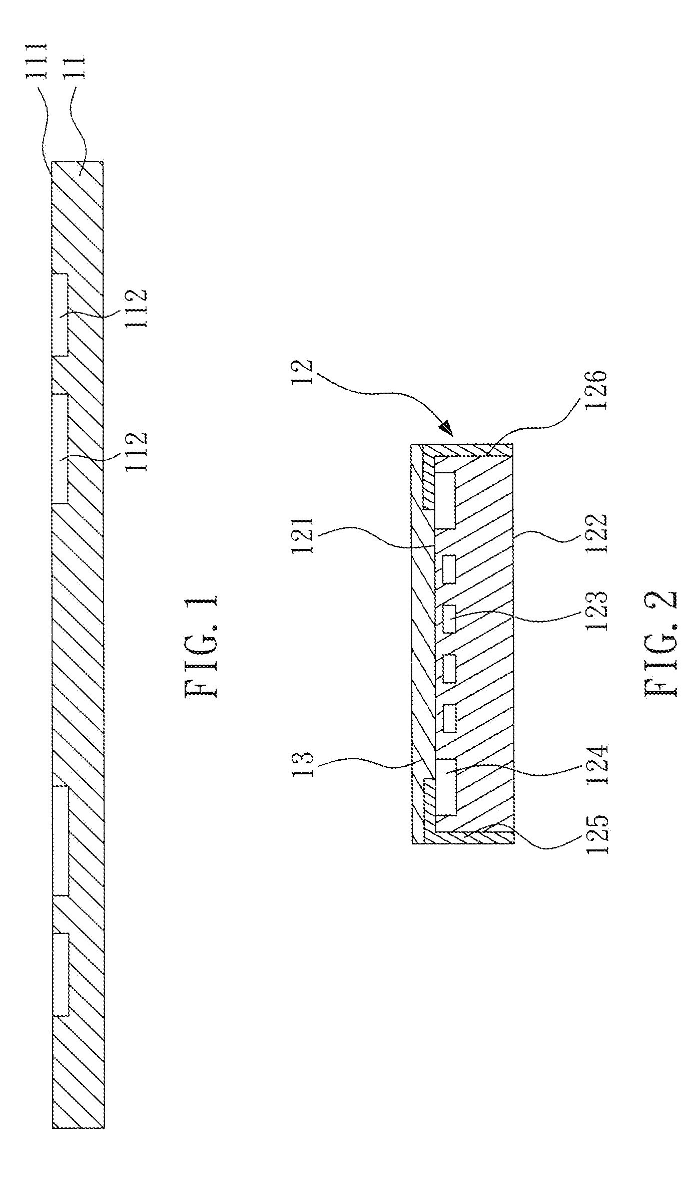
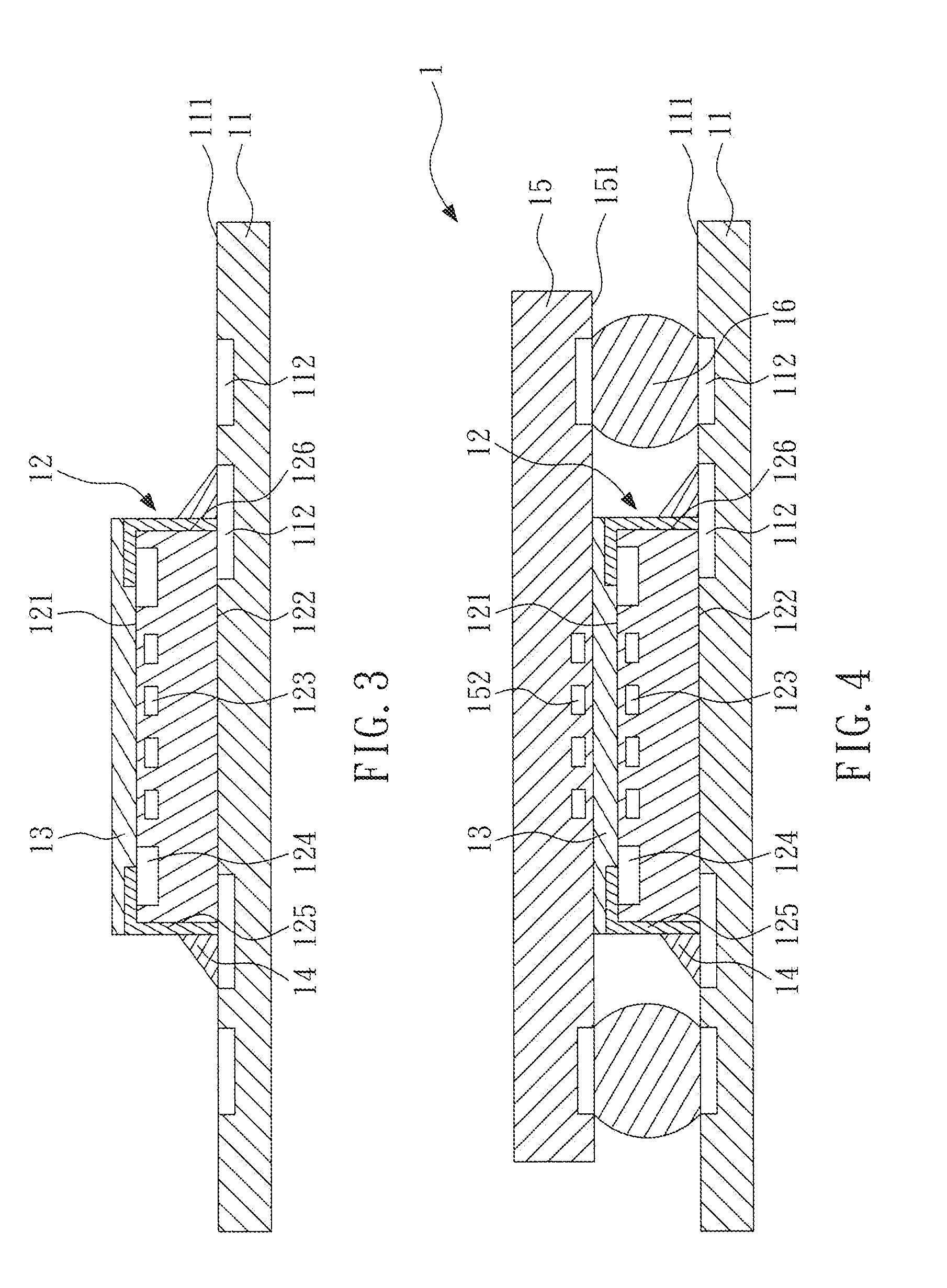
[0013]FIGS. 1 to 5 show schematic views of a method for making a semiconductor package according to a first embodiment of the present invention. As shown in FIG. 1, a substrate 11 is provided. The substrate 11 has a receiving surface 111. In the embodiment, the substrate 11 further comprises a plurality of substrate pads 112 disposed on the receiving surface 111 of the substrate 11.

[0014]As shown in FIG. 2, at least one first chip 12 and a dielectric layer 13 are provided. The first chip 12 has a first active surface 121, a first back surface 122 and a plurality of first signal coupling pads 123. In the embodiment, the first chip 12 further comprises a plurality of first chip pads 124 and a redistribution layer 125. The first signal coupling pads 123 are disposed adjacent to the first active surface 121. The dielectric layer 13 is disposed on the first active surface 121 of the first chip 12. The first chip pads 124 are disposed adjacent to the first active surface 121. The redistri...


PUM


Abstract

The present invention relates to a semiconductor package and a method for making the same. The semiconductor package includes a substrate, at least one first chip, a dielectric layer and at least one second chip. The first chip is attached and electrically connected to the substrate. The first chip includes a first active surface and a plurality of first signal coupling pads. The first signal coupling pads are disposed adjacent to the first active surface. The dielectric layer is disposed on the first active surface. The second chip is attached and electrically connected to the substrate by metal bumps. The second chip includes a second active surface and a plurality of second signal coupling pads. The second active surface contacts the dielectric layer. The second signal coupling pads are disposed adjacent to the second active surface, and capacitively coupled to the first signal coupling pads of the first chip, so as to provide proximity communication between the first chip and the second chip. Whereby, the gap between the first signal coupling pads of the first chip and the second signal coupling pads of the second chip is controlled by the thickness of the dielectric layer. Therefore, the mass-production yield of the semiconductor package is increased.

Description

BACKGROUND OF THE INVENTION[0001]1. Field of the Invention[0002]The present invention relates to a semiconductor package and a method for making the same, and more particularly to a semiconductor package having signal coupling pads and a method for making the same.[0003]2. Description of the Related Art[0004]A new technique referred to as “proximity communication” overcomes the limitations of conductive electrical interconnections by using capacitive coupling to provide communications between two chips. This technique provides higher input / output pads densities than traditional wire-bonding and flip-chip bonding input / output pads (about 100 times greater). To achieve proximity communication, the input / output pads disposed on an active surface of each chip are placed face-to-face, and the gap between the input / output pads of different chips must be controlled with extreme accuracy, which is a big challenge.[0005]Therefore, it is necessary to provide a semiconductor package and a meth...

Claims


Application Information

Patent Timeline
IPC IPC(8): H01L23/48H01L21/50
CPCH01L23/48H01L2224/0401H01L24/13H01L24/16H01L24/29H01L24/32H01L24/33H01L24/73H01L24/81H01L24/83H01L25/0657H01L2224/02371H01L2224/02381H01L2224/14155H01L2224/16225H01L2224/2919H01L2224/2929H01L2224/29294H01L2224/293H01L2224/32105H01L2224/32145H01L2224/32225H01L2224/33183H01L2224/73103H01L2224/73203H01L2224/81191H01L2224/83192H01L2224/83815H01L2224/83851H01L2224/839H01L2225/06517H01L2225/06531H01L2225/06551H01L2225/06555H01L24/02H01L2924/014H01L2224/83903H01L2924/00012
Inventor LAI, YI-SHAOTSAI, TSUNG-YUEHCHEN, MING-KUNCHANG, HSIAO-CHUANCHENG, MING-HSIANG
Owner ADVANCED SEMICON ENG INC
Learn More