Manufacturing method of liquid crystal display device and liquid crystal display device

a liquid crystal display and manufacturing method technology, applied in semiconductor devices, instruments, optics, etc., can solve the problems of deterioration, display properties change, reliability decline, etc., to improve reliability, reduce cost, and improve voltage change over time between a pair of substrates (electrodes).

Inactive Publication Date: 2012-04-19
SEIKO EPSON CORP
View PDF2 Cites 10 Cited by
  • Summary
  • Abstract
  • Description
  • Claims
  • Application Information

AI Technical Summary

Benefits of technology

[0009]An advantage of some aspects of the invention is to provide a liquid crystal display device with improved reliability in which the vol...

Problems solved by technology

In the liquid crystal panel having the above described configuration, improvements of various properties are requested, and the improvement of reliability...

Method used


Image

  • Manufacturing method of liquid crystal display device and liquid crystal display device
  • Manufacturing method of liquid crystal display device and liquid crystal display device
  • Manufacturing method of liquid crystal display device and liquid crystal display device

Examples


experimental example

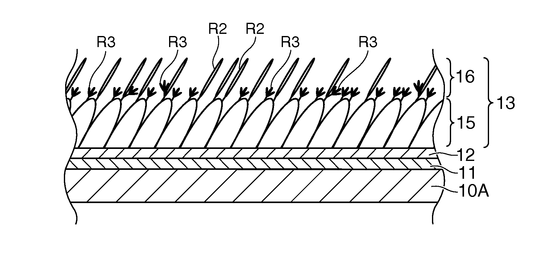
[0077]As a liquid crystal panel according to the invention, a working example product and a comparative example product were fabricated using the same method as the manufacturing method of the above described embodiment.

[0078]Note that, in the manufacturing of the working example product, decyl trimethoxysilane with three hydrolytic groups was used as the first silane coupling agent and trimethyl methoxysilane with one hydrolytic group was used as the second silane coupling agent.

[0079]Further, in the manufacturing of the comparative example product, decyl trimethoxysilane was used as the first silane coupling agent and methyl trimethoxysilane with three hydrolytic groups was used as the second silane coupling agent.

[0080]Aging tests were respectively conducted on the obtained liquid crystal panels of the working example product and the comparative example product.

[0081]Vcom at the start of aging and Vcom at the end of aging (after a predetermined time has elapsed) were respectively...


PUM


Abstract

A manufacturing method of a liquid crystal display device including a liquid crystal layer sandwiched between a pair of opposed substrates and orientation films includes forming a first orientation film having straight-chain alkyl chains at the liquid crystal layer side of one substrate, and forming a second orientation film at the liquid crystal layer side of the other substrate by forming an inorganic orientation layer and surface-treating the inorganic orientation layer using a silane coupling agent, and forming the second orientation film includes surface-treating the inorganic orientation layer using a first silane coupling agent having straight-chain alkyl chains and surface-treating the layer using a second silane coupling agent having straight-chain alkyl chains and having only one hydrolytic group.

Description

BACKGROUND[0001]1. Technical Field[0002]The present invention relates to a manufacturing method of a liquid crystal display device and a liquid crystal display device.[0003]2. Related Art[0004]In related art, liquid crystal panels have been used for many displays (display apparatuses) such as televisions, monitors, and cameras. In the liquid crystal panel (liquid crystal display apparatus), pixel electrodes and a common electrode are formed on a pair of substrates, a liquid crystal layer is sandwiched between the electrodes, and orientation films are respectively formed on the inner surfaces of the respective substrates, i.e., on the liquid crystal layer sides of the respective electrodes.[0005]In the liquid crystal panel having the above described configuration, improvements of various properties are requested, and the improvement of reliability is one of the issues. Particularly, since a liquid crystal panel used for a projector is necessary to be driven with high brightness under...

Claims


Application Information

Patent Timeline
IPC IPC(8): G02F1/1337H01L33/08
CPCG02F1/133719G02F2001/133773G02F1/133734G02F1/133773
Inventor AKAGAWA, TOMOKONAGAE, NOBUKAZU
Owner SEIKO EPSON CORP
Why Eureka
Try Eureka