Signal buffer circuit, sensor control board, image scanner, and image forming apparatus

Inactive Publication Date: 2012-04-19
RICOH KK
View PDF4 Cites 37 Cited by
  • Summary
  • Abstract
  • Description
  • Claims
  • Application Information

AI Technical Summary

Benefits of technology

[0007]In one aspect of the present invention, a signal buffer circuit is devised. A signal buffer circuit includes a buffer to conduct a buffering operation for transmitting a signal to a subsequent unit; a resistor connected between an input side and an output side of the buffer; and a variable impedance device connected in series to the output side of the buffer. The variable impedance device is at low impedance when the buffer is conducting the buffering operation and at high impedance when the buffer is not conducting the buffering operation.
[0008]In another aspect of the present invention, a signal buffer circuit is devised. A signal buffer circuit includes a buffer to conduct a buffering operation for transmitting a signal to a subsequent unit; a first variable impedance device connected between an input side and an output side of the buffer, the first variable impedance device is at a high impedance when the buffer is conducting the buffering operation, a

Problems solved by technology

At this time, during transitional operations, such as power source ON/OFF, or clock input or shutdown, over-output or under-output from the CCD or signal disruption occurs, leading to excess voltage or excess current at the AFE.
Although successful at preventing over-vol

Method used


Image

  • Signal buffer circuit, sensor control board, image scanner, and image forming apparatus
  • Signal buffer circuit, sensor control board, image scanner, and image forming apparatus
  • Signal buffer circuit, sensor control board, image scanner, and image forming apparatus

Examples


Embodiment Construction

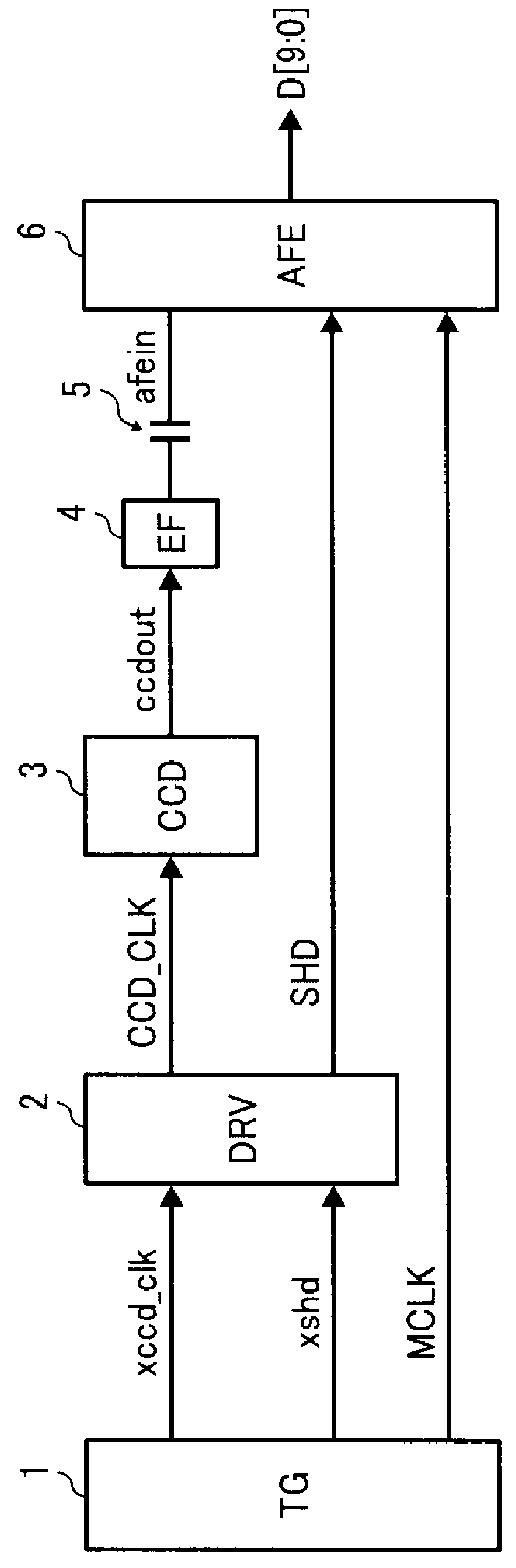
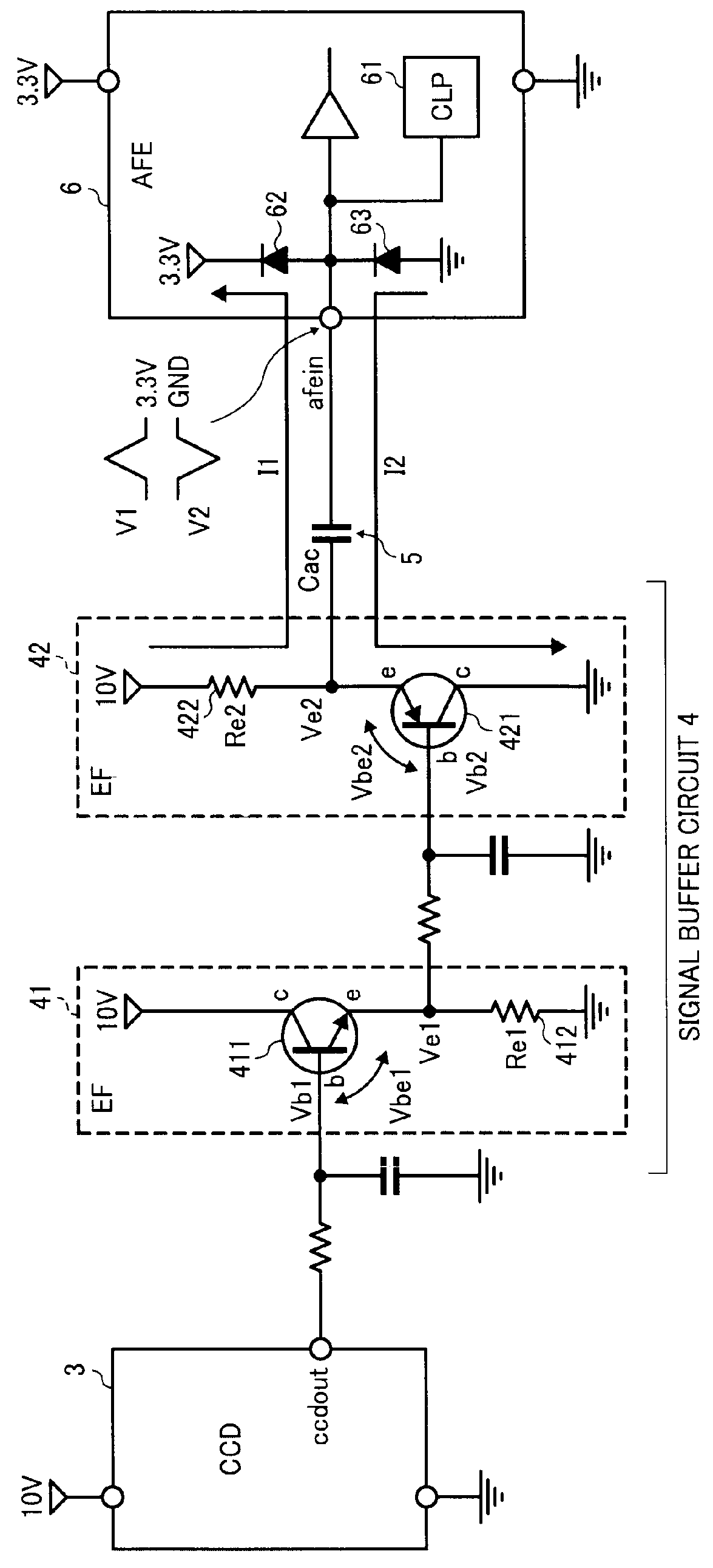
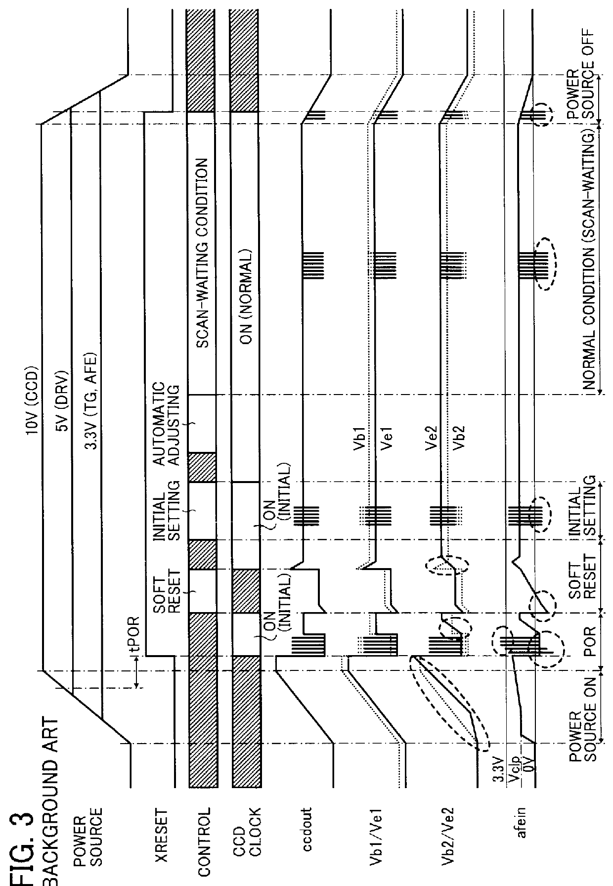
[0035]A description is now given of exemplary embodiments of the present invention. It should be noted that although such terms as first, second, etc. may be used herein to describe various elements, components, regions, layers and / or sections, it should be understood that such elements, components, regions, layers and / or sections are not limited thereby because such terms are relative, that is, used only to distinguish one element, component, region, layer or section from another region, layer or section. Thus, for example, a first element, component, region, layer or section discussed below could be termed a second element, component, region, layer or section without departing from the teachings of the present invention.

[0036]In addition, it should be noted that the terminology used herein is for the purpose of describing particular embodiments only and is not intended to be limiting of the present invention. Thus, for example, as used herein, the singular forms “a”, “an” and “the...


PUM


Abstract

A signal buffer circuit includes a buffer to conduct a buffering operation for transmitting a signal to a subsequent unit; a resistor connected between an input side and an output side of the buffer; and a variable impedance device connected in series to the output side of the buffer. The variable impedance device is at low impedance when the buffer is conducting the buffering operation and at high impedance when the buffer is not conducting the buffering operation.

Description

CROSS-REFERENCE TO RELATED APPLICATIONS[0001]This application claims priority to Japanese Patent Application No. 2010-230829, filed on Oct. 13, 2010 in the Japan Patent Office, which is incorporated by reference herein its entirety.BACKGROUND OF THE INVENTION[0002]1. Field of the Invention[0003]The present invention relates to a signal buffer circuit, a sensor control board including the signal buffer circuit, an image scanner including the signal buffer circuit and sensor control board, and an image forming apparatus including the image scanner.[0004]2. Description of the Background Art[0005]Scanners receive light reflected from a document image face (hereinafter, document), and then the light is photo-electrically converted to electrical signals using an image sensor such as a charge coupled device (CCD) installed in a sensor control board, by which an image of the document is read, or scanned. In the sensor control board, signals output from the CCD are buffered by a signal buffe...

Claims


Application Information

Patent Timeline
IPC IPC(8): H04N1/04H03K3/00
CPCH04N1/00928H04N1/1013H04N2201/0081H04N5/372H04N1/193H04N25/71
Inventor NAKAZAWA, MASAMOTO
Owner RICOH KK
Why Eureka
Try Eureka