Encapsulated circuit device for substrates having an absorption layer, and method for the manufacture thereof

a technology of absorption layer and encapsulation circuit, which is applied in the direction of printed circuit manufacturing, printed circuit non-printed electric component association, and semiconductor/solid-state device details, etc. it can solve the problems of high load in terms of power loss, current intensity and temperature, unreliable electrical contacts, and components, so as to reduce mechanical stresses and reduce mechanical stresses. , the effect of little or no additional required spa

Inactive Publication Date: 2012-04-19
ROBERT BOSCH GMBH
View PDF7 Cites 16 Cited by
  • Summary
  • Abstract
  • Description
  • Claims
  • Application Information

AI Technical Summary

Benefits of technology

[0010]The present invention renders possible an especially space-saving circuit structure that is well protected from external influences and that also functions reliably even at very great temperature differences. In particular, by employing the circuit structure according to the present invention, mechanical stresses, which cause numerous problems, particularly in broad temperature application ranges, may be reduced by several orders of magnitude, the means for reducing the mechanical stresses involving only very little or no additional required space. The circuit is suited, in particular, for substrates and components having large dimensions, in particular for substrates which are substantially thicker than a silicon chip, without any appreciable mechanical stresses being produced, by the large enclosed volume in response to significant temperature variations. In addition, the present invention is suited for reducing mechanical stresses by several orders of magnitude, even when working with significant spatial temperature gradients within the circuit, as occur most notably in relatively large circuits due to heat accumulation. Thus, the present invention also makes it possible for a component, which generates considerable heat, to be mounted on the same substrate as a component, which has a significantly lower temperature, without any gaps or mechanical stresses being produced.
[0021]The absorption layer used for the circuit device, respectively the absorption layer provided by the method is thus preferably a deformable layer, whereas the outer encapsulation forms a hard, in principle elastic and not very flexible outer layer. Thus, the outer encapsulation is a hard material which absorbs externally acting mechanical loads and which, by virtue of its mechanical stability, protects the interior of the component from external mechanical effects. At the same time, the outer encapsulation is mechanically stable, not brittle, and elastically absorbs forces, even at an elasticity modulus that is typically high for hard materials, for example greater than 10 kN / mm2. Both layers preferably feature a high thermal conductivity. It is an aim of the manufacturing method that the morphology of both layers correspond to a non-porous structure. The layers are constituted of continuous solid material that may have individual bubbles that are inherent to the manufacturing, an efficient transfer of heat and a stable mechanical structure being ensured. The absorption layer may have a constant layer thickness or may be provided with a minimum thickness as described above. In particular, the thickness of the absorption layer between the power components and the outer encapsulation preferably corresponds to a minimum of all thicknesses of the layer, to render possible an efficient transfer of heat. At the same time, the thickness provided there preferably corresponds at least to the minimum thickness.

Problems solved by technology

Particularly in the case of power circuits, for example in the automotive sector, the circuit is provided for high-current applications, resulting in high loads in terms of power losses, current intensity and temperature.
However, the described encapsulation by embedding or potting also entails disadvantages since materials having different properties, in particular different coefficients of thermal expansion, come into contact with one another.
This results in unreliable electrical contacts, interruptions, components that are influenced by mechanical stresses during operation thereof, and gap formations.
However, in the automotive sector, in particular, circuits of this kind are used in the engine compartment, very significant temperature fluctuations usually occurring there.

Method used


Image

  • Encapsulated circuit device for substrates having an absorption layer, and method for the manufacture thereof
  • Encapsulated circuit device for substrates having an absorption layer, and method for the manufacture thereof
  • Encapsulated circuit device for substrates having an absorption layer, and method for the manufacture thereof

Examples


Embodiment Construction

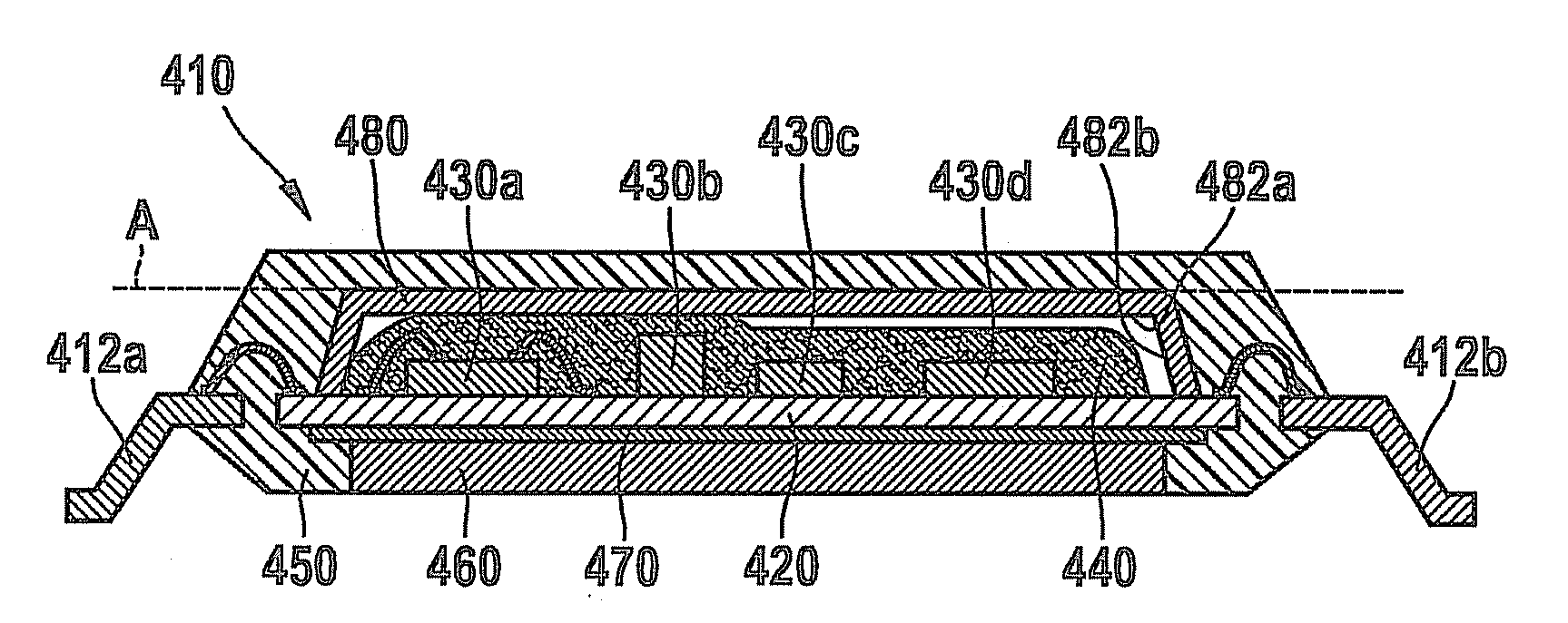
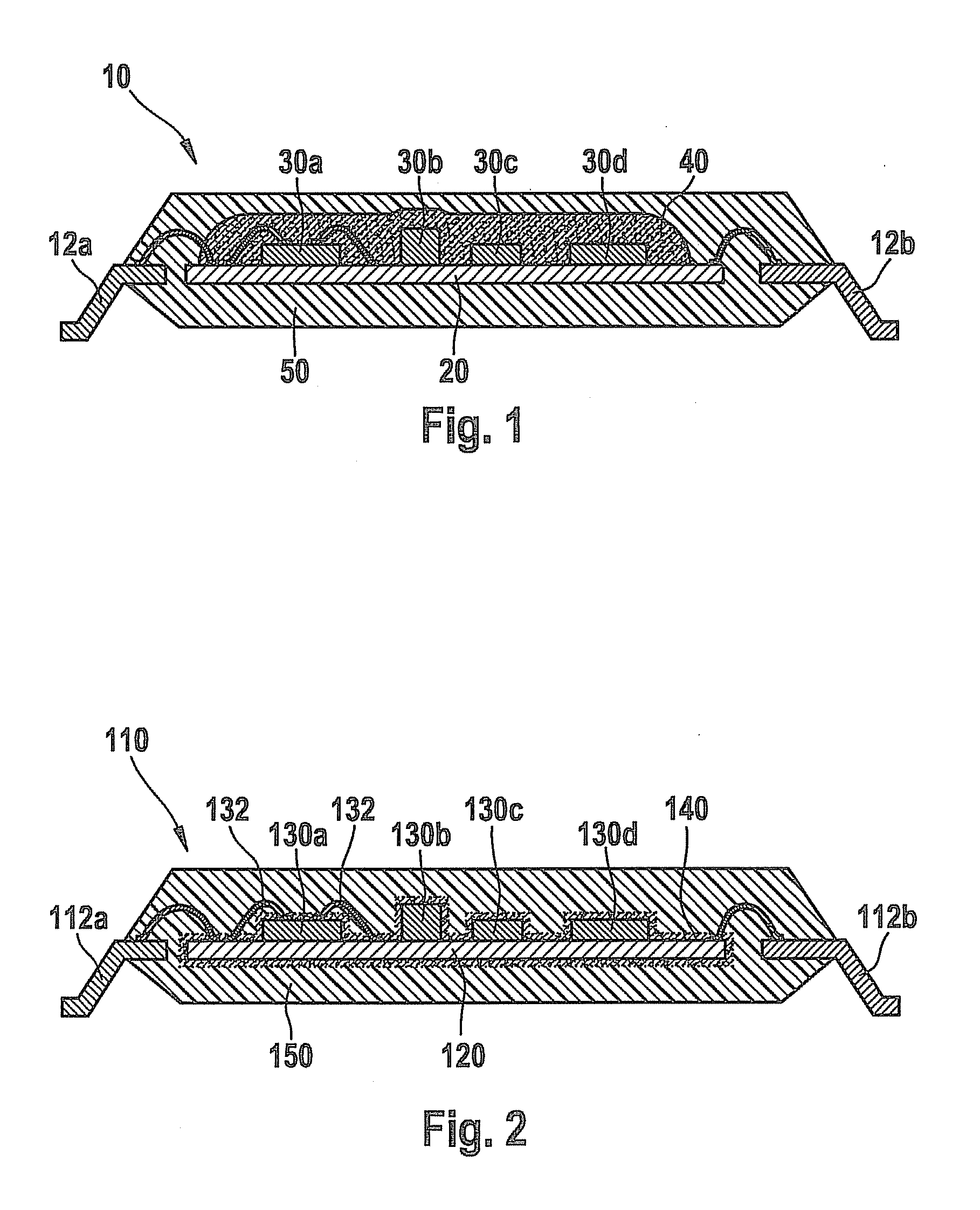
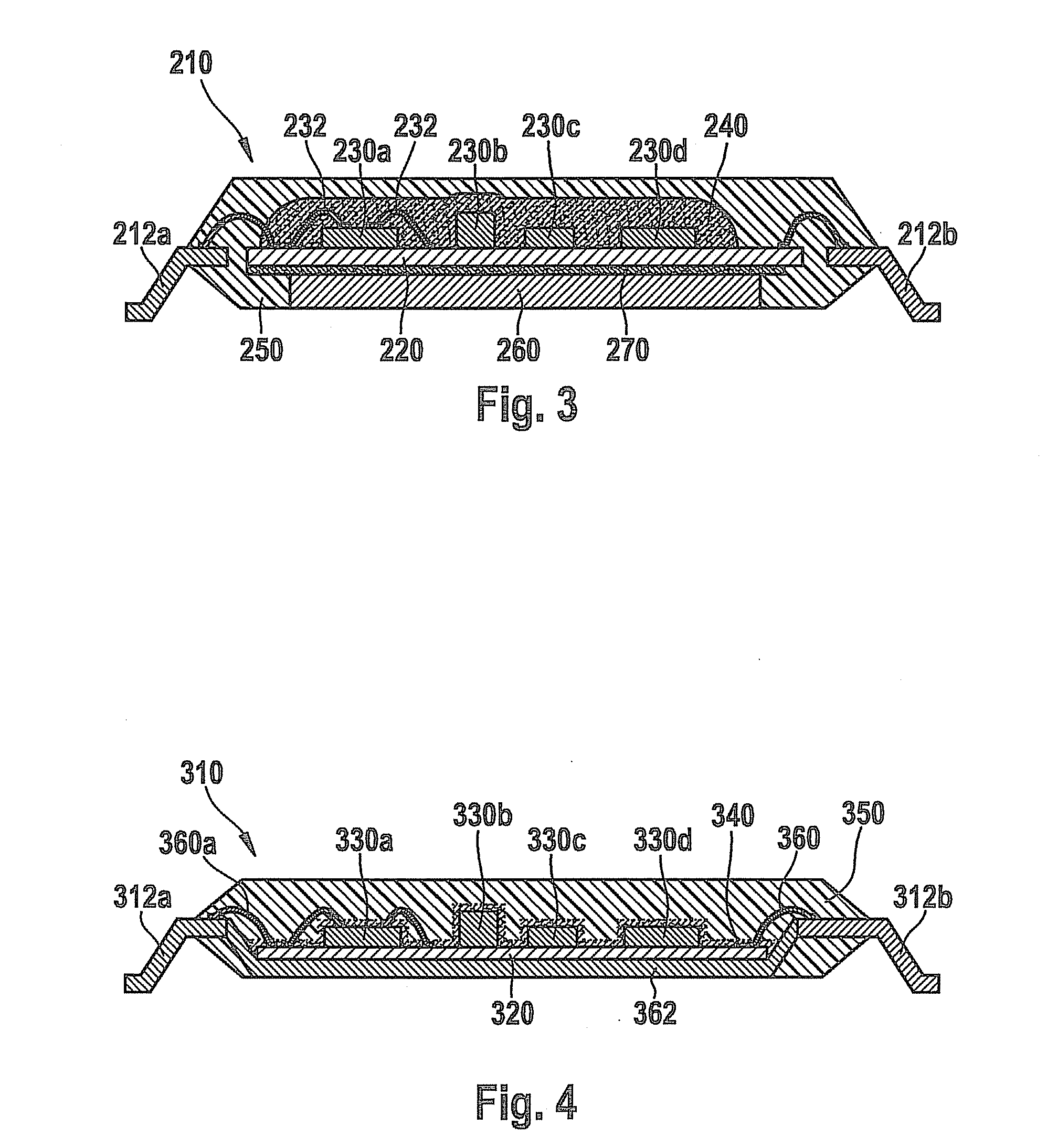
[0031]FIG. 1 shows a circuit device 10 according to the present invention that includes electrical contacts 12a,b. Circuit device 10 encompasses a substrate 20 on which components 30a-d are provided. SMD soldering techniques or an electrically conductive adhesive are / is used to mount components 30a-d on the component side of substrate 20 which bears a patterned conductor layer. All components 30a-d are surrounded by a compressible absorption layer 40, which completely covers the components, as well as a portion of the component side of the substrate surface. On the one side, the absorption layer covers a connection to the electrical contact 12a (i.e., a bonding connection to the substrate), whereas the connection to contact 12b provided on the substrate is not covered by the absorption layer. The absorption layer does not cover the complete component side of substrate 20. Rather an edge remains between the covered substrate surface portion and the complete component side on which el...


PUM

PropertyMeasurementUnit
thicknessaaaaaaaaaa
thicknessaaaaaaaaaa
thicknessaaaaaaaaaa

Abstract

An encapsulated circuit device has a substrate, components configured on a substrate surface portion of a component side of the substrate, an encapsulation, at least one electrical contact having an outer portion projecting out of the encapsulation and an inner portion provided in the circuit device that is electrically connected to the substrate. The encapsulation includes a rigid outer encapsulation, which extends completely around the substrate, the components and the inner portion of the at least one electrical contact, as well as a compressible deformation absorption layer, which is provided between the components and the outer encapsulation and at least completely covers the substrate surface portion on which the components are configured.

Description

BACKGROUND OF THE INVENTION[0001]1. Field of the Invention[0002]The present invention relates to substrate-based circuits and, in particular, to circuits having a plurality of discrete or integrated components that are provided on the substrate.[0003]2. Description of Related Art[0004]In the case of substrate-based or printed circuit board-based circuits, a multiplicity of individual discrete or integrated components are affixed to a substrate, which, on the one hand, provides an electrical connection among the components and, on the other hand, provides a mechanical support. An insulation layer serves as a support for a circuit-board conductor layer whose structure defines the electrical connections of the electrical components. This circuit technology differs in principle from integrated circuits where a single silicon chip provides both a substrate, as well as all components, i.e., no components are mounted on the substrate.[0005]Particularly in the case of power circuits, for ex...

Claims


Application Information

Patent Timeline
Patent Type & Authority Applications(United States)
IPC IPC(8): H05K1/18H05K3/30
CPCH01L23/3107H01L2924/30107H01L23/3135H01L23/4334H01L23/49531H01L2224/48091H01L2224/48247H01L2924/01004H01L2924/0102H01L2924/09701H01L2924/19041H05K3/284H05K2203/1322Y10T29/49146H01L2924/1301H01L24/48H01L2924/19107H01L2924/10253H01L23/3121H01L2924/00014H01L2924/00H01L2924/13033H01L2924/14H01L2924/181H01L2924/00012H01L2224/45099H01L2224/45015H01L2924/207
Inventor NEUMEISTER, JOCHENRIEGER, REINHARD
Owner ROBERT BOSCH GMBH
Why Eureka
Try Eureka