Method for forming semiconductor device

a semiconductor and device technology, applied in the direction of semiconductor devices, basic electric elements, electrical appliances, etc., can solve the problems of worsening of storage operation characteristics

Active Publication Date: 2012-04-26
LONGITUDE LICENSING LTD
View PDF4 Cites 25 Cited by
  • Summary
  • Abstract
  • Description
  • Claims
  • Application Information

AI Technical Summary

Problems solved by technology

If the contact plugs that are disposed in the memory cell region and directly connected to the semiconductor substrate are formed from metal, there has been concern with a worsening of storage operation characteristics, caused by the influence of an increase in the junction leakage current or the like.

Method used


Image

  • Method for forming semiconductor device
  • Method for forming semiconductor device
  • Method for forming semiconductor device

Examples


first embodiment

[0135]A first embodiment of a method for forming a semiconductor device according to the present invention is described below.

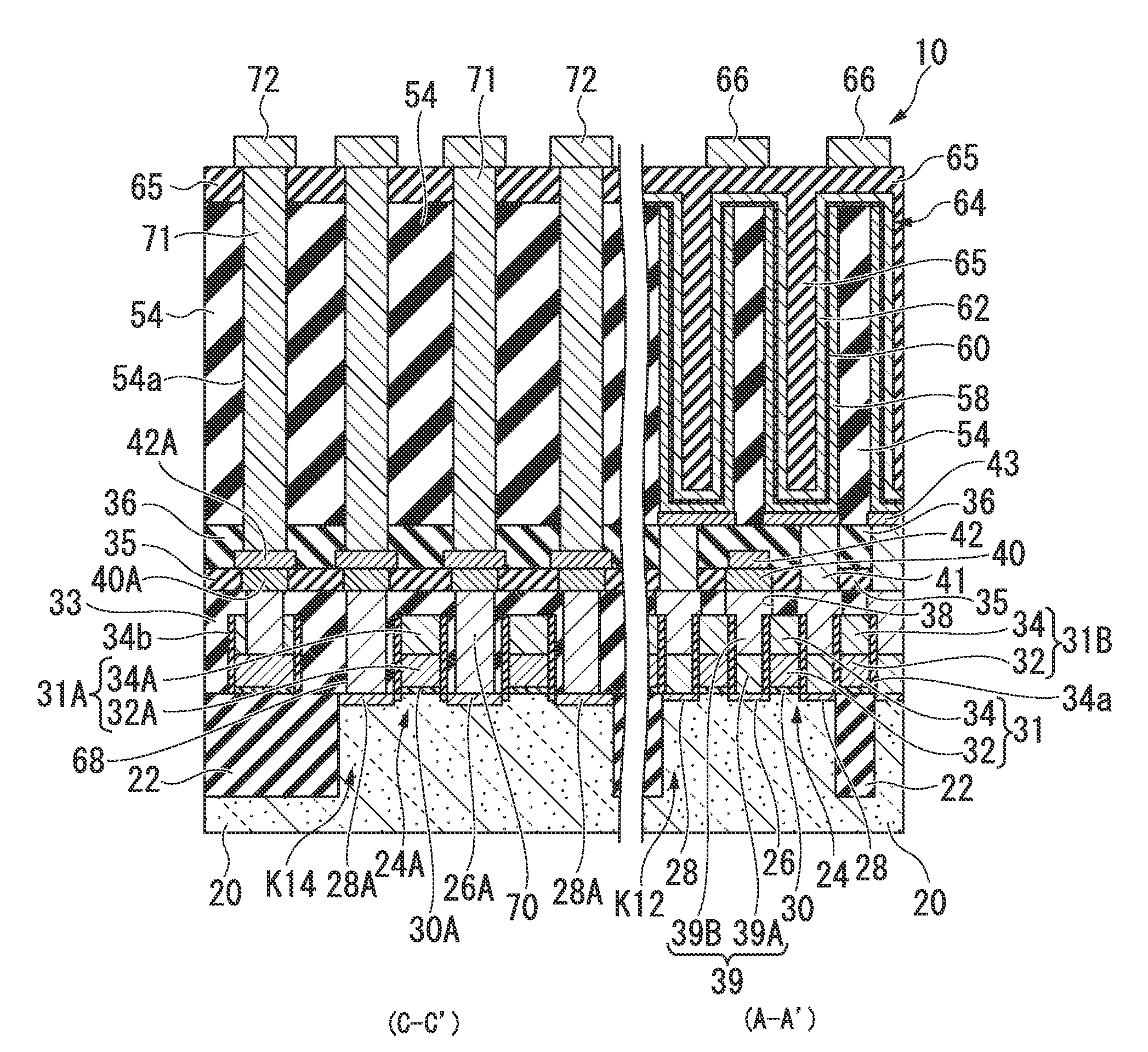
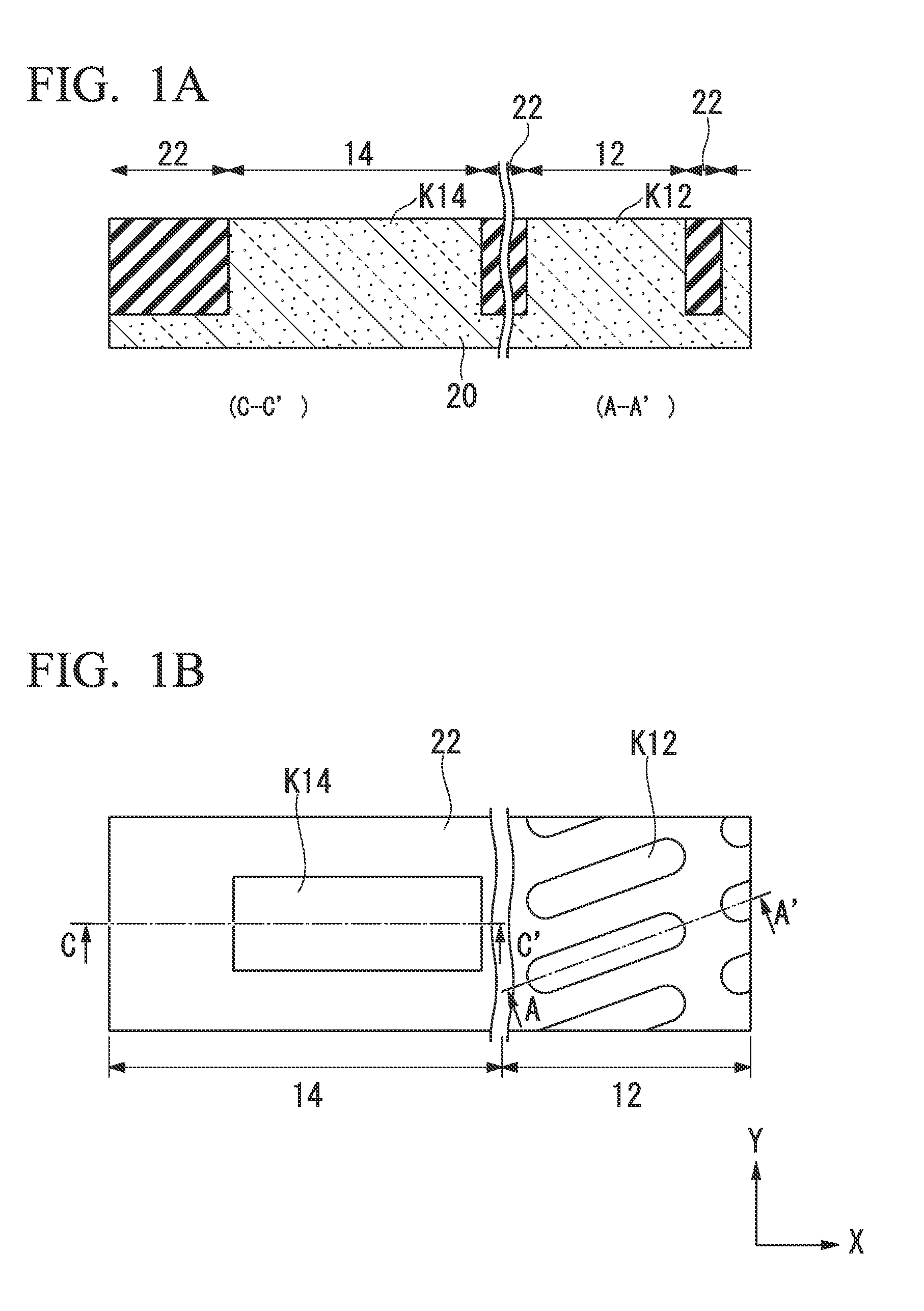
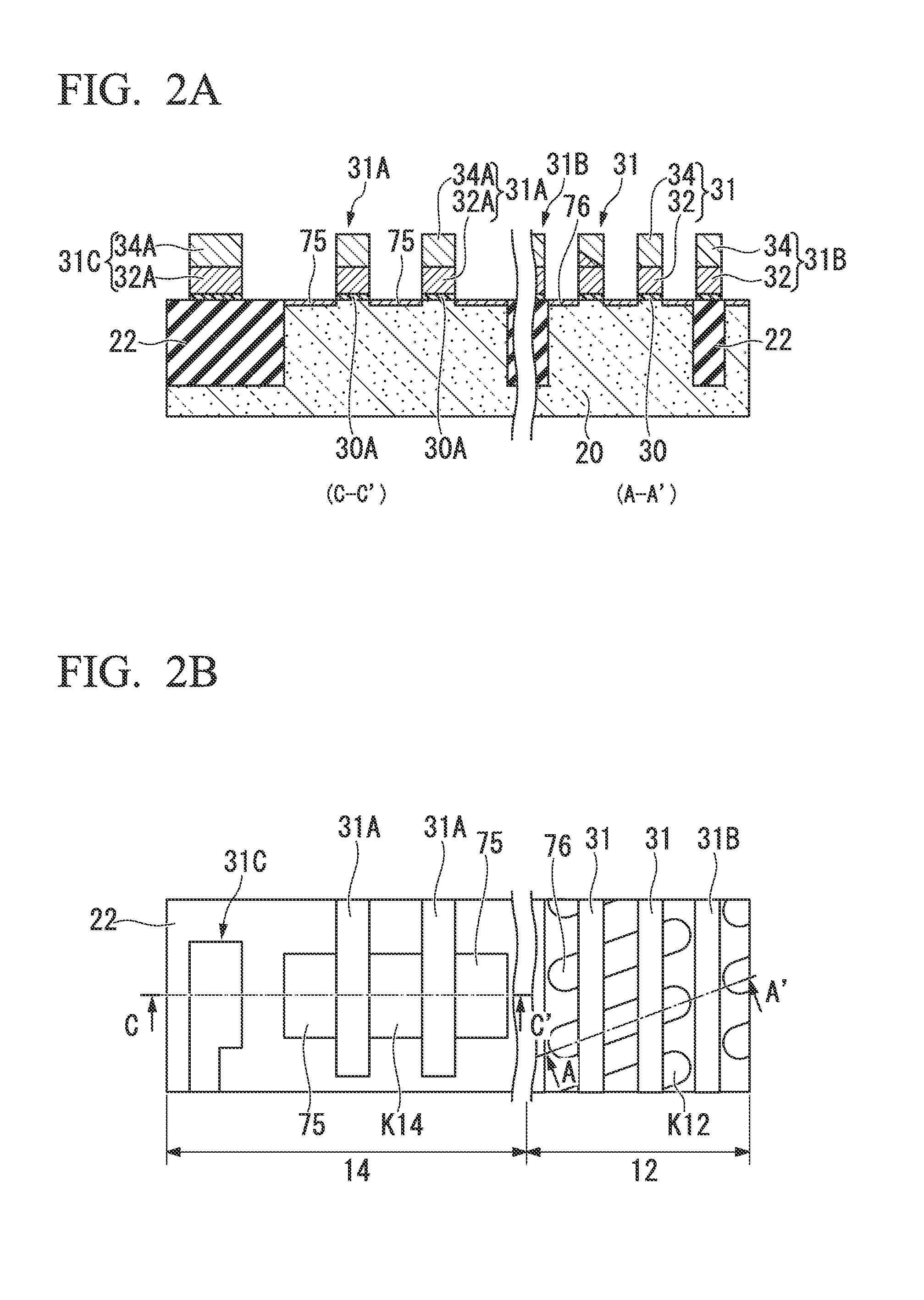
[0136]FIGS. 1A, 2A, 3A, 4A, 5A, 6, 7A, 8A, 9A, 10, 11A, 12A, 13A, and 14A are fragmentary cross sectional elevation views illustrating a semiconductor device in steps involved in a method of forming the semiconductor device in accordance with one embodiment of the present invention. FIGS. 1B, 2B, 3B, 4B, 5B, 7B, 8B, 9A, 11B, 12B, 13B, and 14B are fragmentary plan views illustrating the semiconductor device in steps involved in the method of forming the semiconductor device in accordance with one embodiment of the present invention. An example of this embodiment is that a semiconductor (storage) device 10 as a DRAM element having the cross-sectional structure shown in FIG. 14A can be formed by embodying the method for forming described below based on FIG. 1A to FIG. 14B.

[0137]Before describing the method for forming the semiconductor device according to the pr...

second embodiment

[0215]FIGS. 15A, 15B, 16A, 16B, 17A, 17B, 18A, 18B, 19A, 19B, 20A, 20B, 21A, 21B, 22A, 22B, 23A, 23B, 24A, and 24B are fragmentary cross sectional elevation views illustrating a semiconductor device in steps involved in a method of forming the semiconductor device in accordance with another embodiment of the present invention. FIGS. 15C, 16C, 18C, 19C, 20C, 22C, 23C, and 24C are fragmentary plan views illustrating the semiconductor device in steps involved in the method of forming the semiconductor device in accordance with another embodiment of the present invention. According to the present embodiment, a semiconductor (storage) device 100 as a DRAM element having the cross-sectional structure shown in FIG. 25 can be formed by embodying the method for forming described below, based on FIG. 15A to FIG. 24C.

[0216]Because the semiconductor (storage) device 100 which is formed in the present embodiment includes the same structure as the semiconductor device 10 in the above-noted first ...

third embodiment

[0239]FIGS. 26A, 27A, 28A, 28B, 29A, 29B, 30A, 30B, 31A, 31B, 32A, 32B, 33A, 33B, 34A, 34B, 35A, 35B, 36A, 36B, 37A, 37B, 38A, 38B, and 39A are fragmentary cross sectional elevation views illustrating a semiconductor device in steps involved in a method of forming the semiconductor device in accordance with still another embodiment of the present invention. FIGS. 26B, 27B, 28C, 29C, 30C, 31C, 32C, 33C, 34C, 35C, 36C, 37C, 38C, and 39B are fragmentary plan views illustrating the semiconductor device in steps involved in the method of forming the semiconductor device in accordance with still another embodiment of the present invention. A semiconductor (storage) device 200 as a DRAM element having the cross sectional structure shown in FIG. 39A can be formed by embodying the method for forming described below, based on FIG. 26A to FIG. 39B.

[0240]Because the semiconductor (storage) device 200 that is formed in the present embodiment includes the same structure as the semiconductor devic...


PUM


Abstract

A method of forming a semiconductor device includes the following processes. A first interlayer insulating film is formed over a cell transistor and a peripheral transistor. A cell contact hole is formed in the first interlayer insulating film, the cell contact hole reaching the cell transistor. A lower contact plug is formed at a bottom of the cell contact hole. A peripheral contact hole is formed in the first interlayer insulating film, the peripheral contact hole reaching the peripheral transistor. A first peripheral contact plug is simultaneously formed in the peripheral contact hole and an upper contact plug in the cell contact hole, the upper contact plug being disposed on the lower contact plug.

Description

BACKGROUND OF THE INVENTION[0001]1. Field of the Invention[0002]The present invention generally relates to a method for forming a semiconductor device.[0003]Priority is claimed on Japanese Patent Application No. 2010-236488, filed Oct. 21, 2010, the content of which is incorporated herein by reference.[0004]2. Description of the Related Art[0005]Japanese Unexamined Patent Application, First Publication, No. JP-A-2002-009174 discloses a semiconductor device which has a memory cell region, such as a DRAM. Japanese Unexamined Patent Application, First Publications, Nos. JP-A-2002-009174 also discloses a technique in which storage elements (for example, capacitors) disposed in the memory cell region and MOS transistors used for selecting are connected via a plurality of contact plugs.[0006]With advances in the microstructuring of semiconductor devices, because the size of contact plugs disposed in the memory cell region has also been shrinking, the operational characteristics tend to be...

Claims


Application Information

Patent Timeline
Patent Type & Authority Applications(United States)
IPC IPC(8): H01L21/336H01L21/768H01L21/28
CPCH01L21/76816H01L21/76897H01L27/10894H01L27/10888H01L27/10855H10B12/0335H10B12/485H10B12/09
Inventor SAKO, NOBUYUKIHASUNUMA, EIJI
Owner LONGITUDE LICENSING LTD
Why Eureka
Try Eureka