
Semiconductor light emitting device

Active Publication Date: 2012-05-03
SAMSUNG ELECTRONICS CO LTD
View PDF3 Cites 4 Cited by
  • Summary
  • Abstract
  • Description
  • Claims
  • Application Information

AI Technical Summary

Benefits of technology

[0009]An aspect of the present invention provides a semiconductor light emitting device having electrodes for minimizing a loss of light and improving a current spreading effect.

Problems solved by technology

The narrow current flow increases an operation voltage Vf of the light emitting device, degrading current efficiency, and in addition, the light emitting device may become vulnerable to an electrostatic discharge.
Thus, the area of the active layer is reduced and a uniform space between the electrodes cannot be secured to cause non-uniform current spreading.

Method used


Image

  • Semiconductor light emitting device
  • Semiconductor light emitting device
  • Semiconductor light emitting device

Examples


Embodiment Construction

[0034]Exemplary embodiments of the present invention will now be described in detail with reference to the accompanying drawings.

[0035]The invention may, however, be embodied in many different forms and should not be construed as being limited to the embodiments set forth herein. Rather, these embodiments are provided so that this disclosure will be thorough and complete, and will fully convey the scope of the invention to those skilled in the art. In the drawings, the shapes and dimensions may be exaggerated for clarity, and the same reference numerals will be used throughout to designate the same or like components.

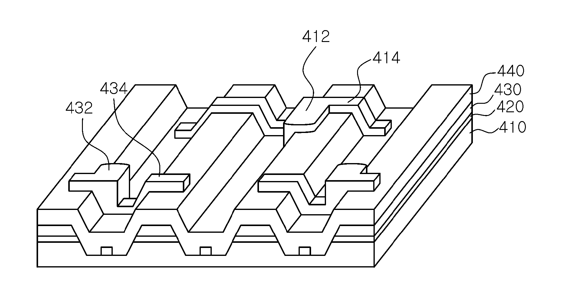
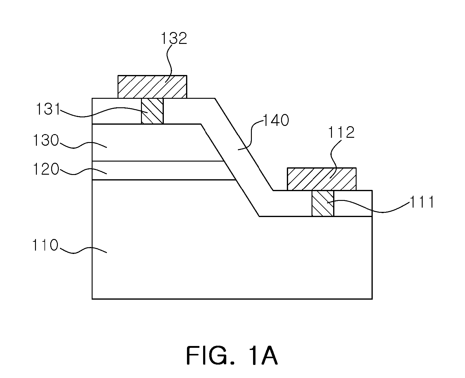
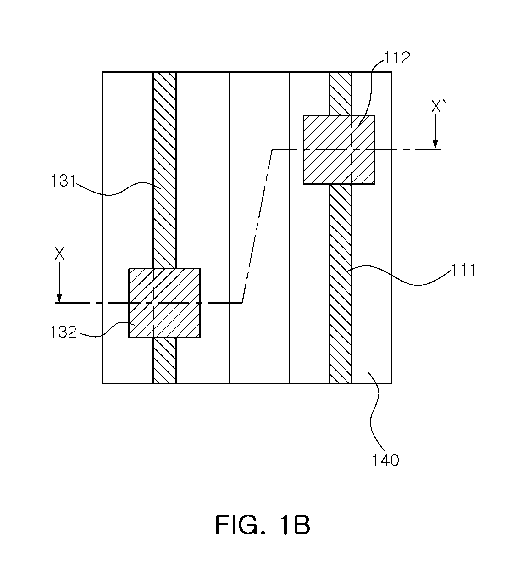
[0036]FIGS. 1a and 1b are a schematic sectional view and a plan view of a semiconductor light emitting device according to an exemplary embodiment of the present invention. Specifically, FIG. 1a is a sectional view taken along line X-X′ in FIG. 1b.

[0037]With reference to FIGS. 1a and 1b, a semiconductor light emitting device according to the present exemplary embodimen...


PUM


Abstract

A semiconductor light emitting device includes: a first conductive semiconductor layer including first and second areas; an active layer disposed on the second area; a second conductive semiconductor layer disposed on the active layer; first and second electrode branches disposed on the first and second conductive semiconductor layers, respectively; a first electrode pad electrically connected to the first electrode branch and disposed on the first electrode branch; and a second electrode pad electrically connected to the second electrode branch and disposed on the second electrode branch.

Description

CROSS-REFERENCE TO RELATED APPLICATIONS[0001]This application claims the priority of Korean Patent Application No. 10-2010-0107809 filed on Nov. 1, 2010, in the Korean Intellectual Property Office, the disclosure of which is incorporated herein by reference.BACKGROUND OF THE INVENTION[0002]1 Field of the Invention[0003]The present invention relates to a semiconductor light emitting device.[0004]2. Description of the Related Art[0005]A light emitting diode, a type of semiconductor light emitting device, is a semiconductor device capable of generating light of various colors according to electron hole recombination in p and n type semiconductor junction parts when current is applied thereto. Compared with a light emitting device based on a filament, the semiconductor light emitting device has various advantages such as a long life span, low power consumption, excellent initial driving characteristics, high vibration resistance, and the like, so demand for the semiconductor light emitt...

Claims


Application Information

Patent Timeline
IPC IPC(8): H01L33/62
CPCH01L27/153H01L33/08H01L33/20H01L33/62H01L33/387H01L33/42H01L33/44H01L33/38H01L33/382
Inventor RYU, YUNG HOHWANG, HAE YEONSHIN, YOUNG CHUL
Owner SAMSUNG ELECTRONICS CO LTD
Features
  • Generate Ideas
  • Intellectual Property
  • Life Sciences
  • Materials
  • Tech Scout
  • Unparalleled Data Quality
  • Higher Quality Content
  • 60% Fewer Hallucinations
Learn More