
Integrated circuit manufacturing method and semiconductor integrated circuit

Inactive Publication Date: 2012-05-03
PANASONIC CORP
View PDF4 Cites 6 Cited by
  • Summary
  • Abstract
  • Description
  • Claims
  • Application Information

AI Technical Summary

Benefits of technology

[0012]The present invention has been conceived in view of the above problems. A purpose of the present invention is to provide an integrated circuit manufacturing method using a layout design method that reduces cost even when the determination of the placement of the external terminals is delayed, and a semiconductor integrated circuit manufactured by the integrated circuit manufacturing method.Solution to Problem
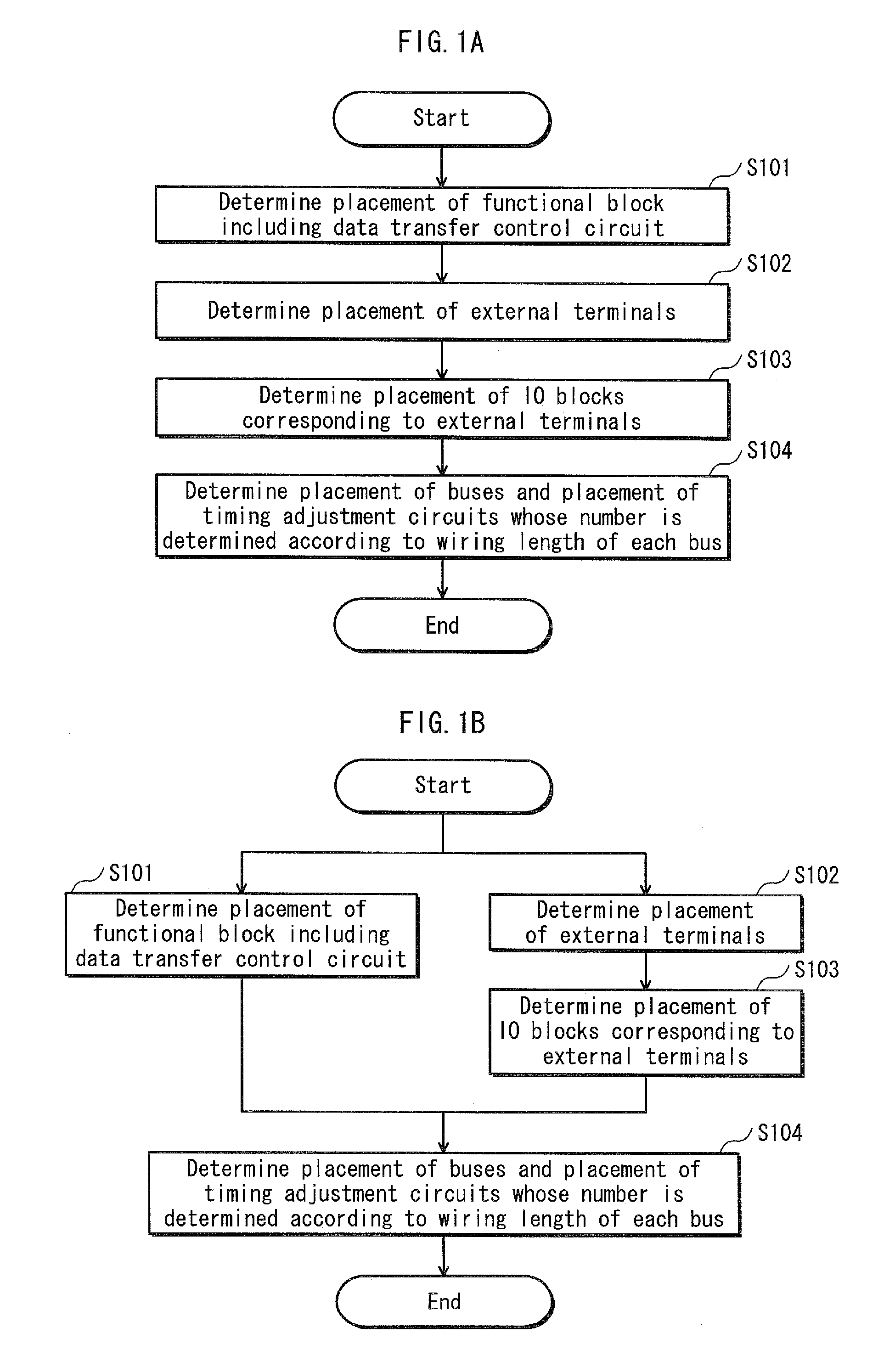
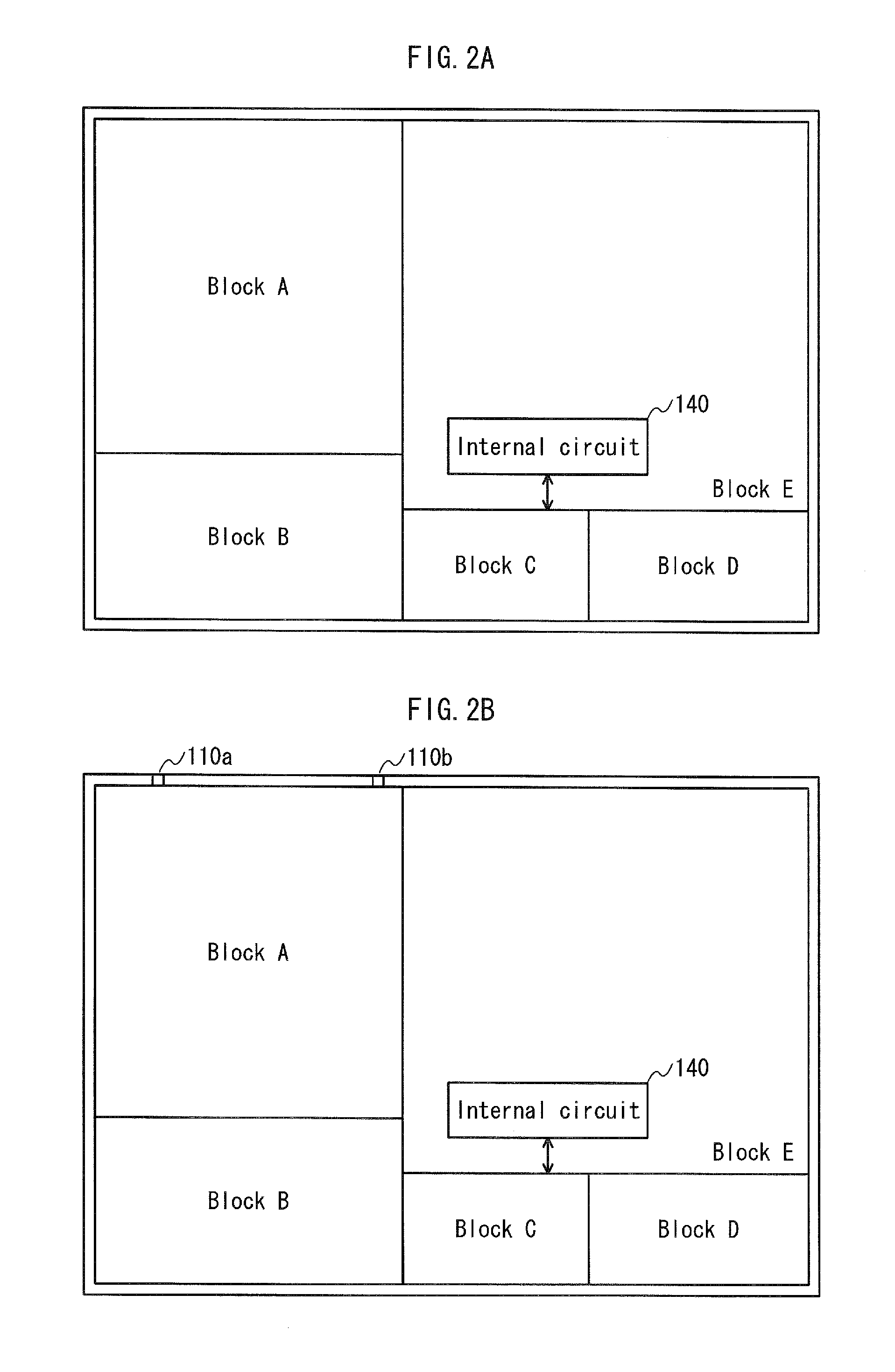
[0014]With the above-mentioned configuration, when the placement of the external terminals is determined after the placement of each functional block and wiring are determined, the placement of the IO blocks (also, referred to as IO cores) is determined such that each IO block corresponds to any of the external terminals. Therefore, it becomes unnecessary to take into account timing adjustment in data transfer between the IO block and the external terminal. Furthermore, by inserting the timing adjustment circuits into the wiring connecting the IO block to the data transfer control circuit according to the wiring length, the transfer delay is prevented. By going through the first, second, third and fourth steps described above, layout design of the functional block is performed without determining the placement of the external terminals. When the placement of the external terminals is determined, the layout design of the semiconductor integrated circuit is performed without changing the placement of each functional block and the like.

Problems solved by technology

In addition, complexity of uses of the external terminal has tended to increase (tendency of a single external terminal to have a plurality of functions has increased) in recent years, and thus determination of the placement of the external terminals has tended to be delayed.
Due to a signal transfer delay occurring by an increase in wiring length, a signal may not be input at an appropriate timing.

Method used


Image

  • Integrated circuit manufacturing method and semiconductor integrated circuit
  • Integrated circuit manufacturing method and semiconductor integrated circuit
  • Integrated circuit manufacturing method and semiconductor integrated circuit

Examples


embodiment 1

[0051]Embodiment 1 describes the layout design method for a semiconductor integrated circuit with reference to a flow chart of FIG. 1A.

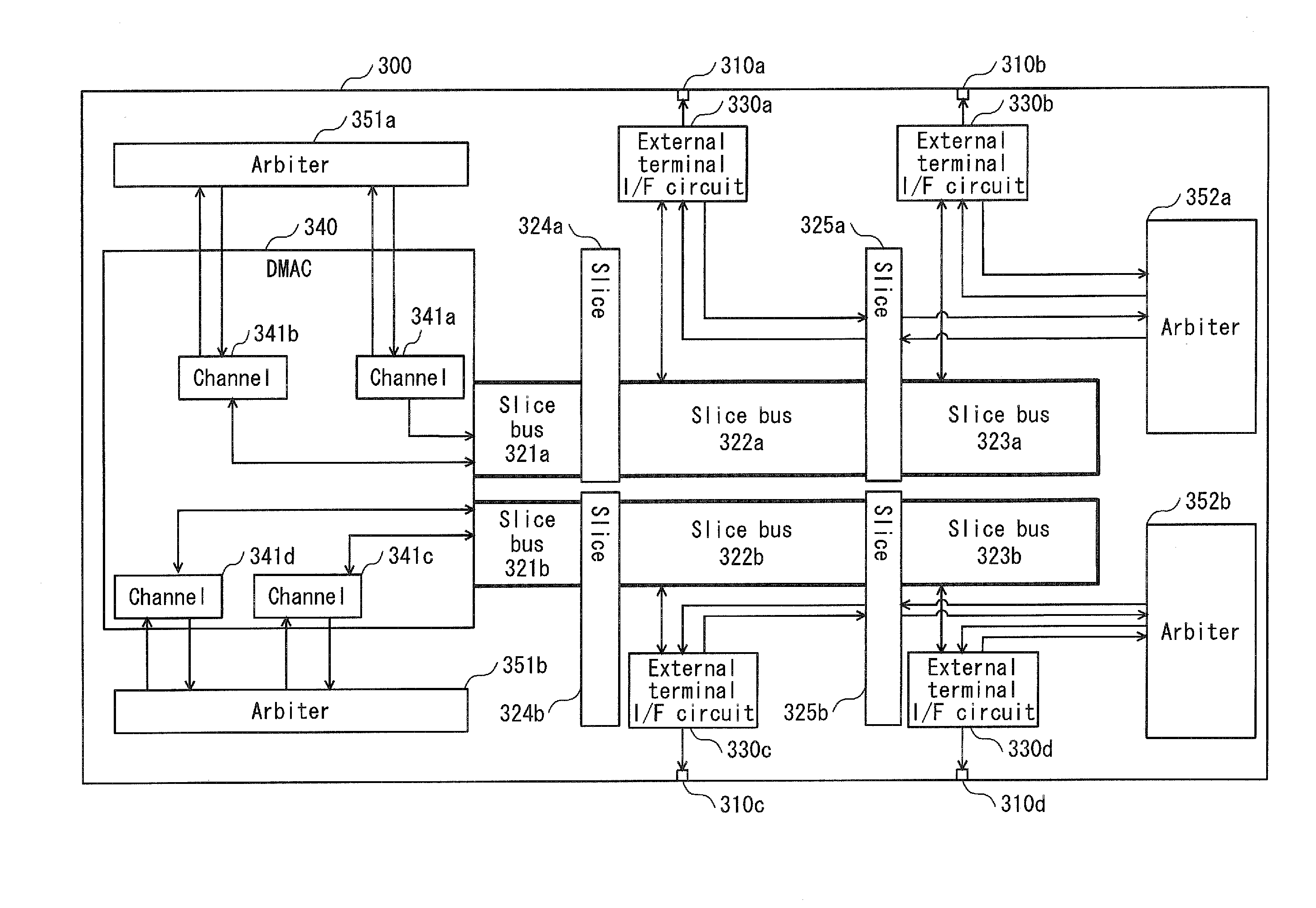
[0052]As shown in FIG. 1A, in the layout design method for a semiconductor integrated circuit in Embodiment 1, placement of functional blocks including a data transfer control circuit is determined at first (step S101). The functional blocks are determined according to a specification required for the semiconductor integrated circuit. The data transfer control circuit has a function of performing data transfer with a circuit and a device to which the designed semiconductor integrated circuit is to be connected. The data transfer control circuit is, for example, a DMAC (Direct Memory Access Controller). That is to say, the data transfer control circuit is a circuit having a master function of the data transfer.

[0053]With such a configuration, design within the semiconductor integrated circuit is completed even if placement of external terminals is not...

modification 1

[0068]In the layout design method in Embodiment 1, the layout design is performed so as to provide the buses for connecting each of the external terminal I / F circuits to the internal circuit. With this structure, however, it is necessary to provide as many buses as the external terminal I / F circuits. There is a problem that an area of the semiconductor integrated circuit increases accordingly.

[0069]In order to solve the above-presented problem, Modification 1 discloses a layout design method that can reduce the area of the semiconductor integrated circuit, compared with the method in Embodiment 1 described above.

[0070]Modification 1 is different from Embodiment 1 in that the bus is not provided for each external terminal I / F circuit, but a shared bus is used to connect the external terminal I / F circuits.

[0071]FIG. 4A is a flow chart showing a layout design method pertaining to Modification 1.

[0072]The layout design method shown in the flow chart of FIG. 4A is different from the meth...

modification 2

[0084]Modification 1 described above presents the layout design using the shared bus as the bus connecting each of the external terminal I / F circuits to the internal circuit. Modification 2 presents a more convenient layout design method.

[0085]Modification 2 is different from Modification 1 described above in timing of determining the placement of the shared bus. That is to say, Modification 2 is different from Modification 1 in that the placement of the shared bus is determined before the placement of the external terminals is determined.

[0086]FIGS. 6A and 6B are each flow charts showing the layout design method pertaining to Modification 2.

[0087]As shown in the flow chart of FIG. 6A, a size of a semiconductor integrated circuit is determined first according to a specification required for the semiconductor integrated circuit to be designed, and then placement of the shared bus is determined. Then, placement of the timing adjustment circuits for adjusting timing of signals flowing ...


PUM


Abstract

In layout design step of the semiconductor integrated circuit manufacturing method, when it is found that the wiring length between an external terminal and an IO block (external terminal I / F circuit) corresponding to the external terminal increases after a floorplan of a circuit including a functional block and the IO block is determined, placement of the IO block is determined such that the IO block is placed close to the external terminal to alleviate constraints on the wiring between the IO block and the external terminal, and timing adjustment circuits whose number is determined according to the wiring length of a bus (or a shared bus) connecting a data transfer circuit and the IO block is inserted into the bus.

Description

TECHNICAL FIELD[0001]The present invention relates to a semiconductor integrated circuit and a method for manufacturing the semiconductor integrated circuit, and in particular, relates to layout design of circuit components.BACKGROUND ART[0002]A process of designing a semiconductor integrated circuit has been divided into two major steps, i.e., front-end design and back-end design. The front-end design is a step of creating a netlist by going through steps such as design of specifications for a semiconductor integrated circuit, functional design, test design and logic synthesis. On the other hand, the back-end design is a step of creating manufacturing data to be used in a manufacturing step by going through steps such as layout design and sign-off verification.[0003]The layout design is further divided into two steps, i.e., floorplanning and wiring planning. The floorplanning is a step of determining placement of various blocks within the semiconductor integrated circuit such as a ...

Claims


Application Information

Patent Timeline
IPC IPC(8): G06F17/50
CPCH01L27/0207
Inventor IWAHASHI, DAISUKETOJIMA, MASAYOSHIKIYOHARA, TOKUZO
Owner PANASONIC CORP
Learn More