

Semiconductor device
a semiconductor memory and semiconductor technology, applied in solid-state devices, capacitors, instruments, etc., can solve the problems of data not being written to a memory element after data is repeatedly written, data loss by electrical charge leakage, power consumption is high, etc., to achieve the effect of suppressing the increase in the number of manufacturing steps and prolonging the data retention period in the semiconductor device or the semiconductor memory devi
- Summary
- Abstract
- Description
- Claims
- Application Information
AI Technical Summary
Benefits of technology
Problems solved by technology
Method used
Image

Examples
embodiment 1
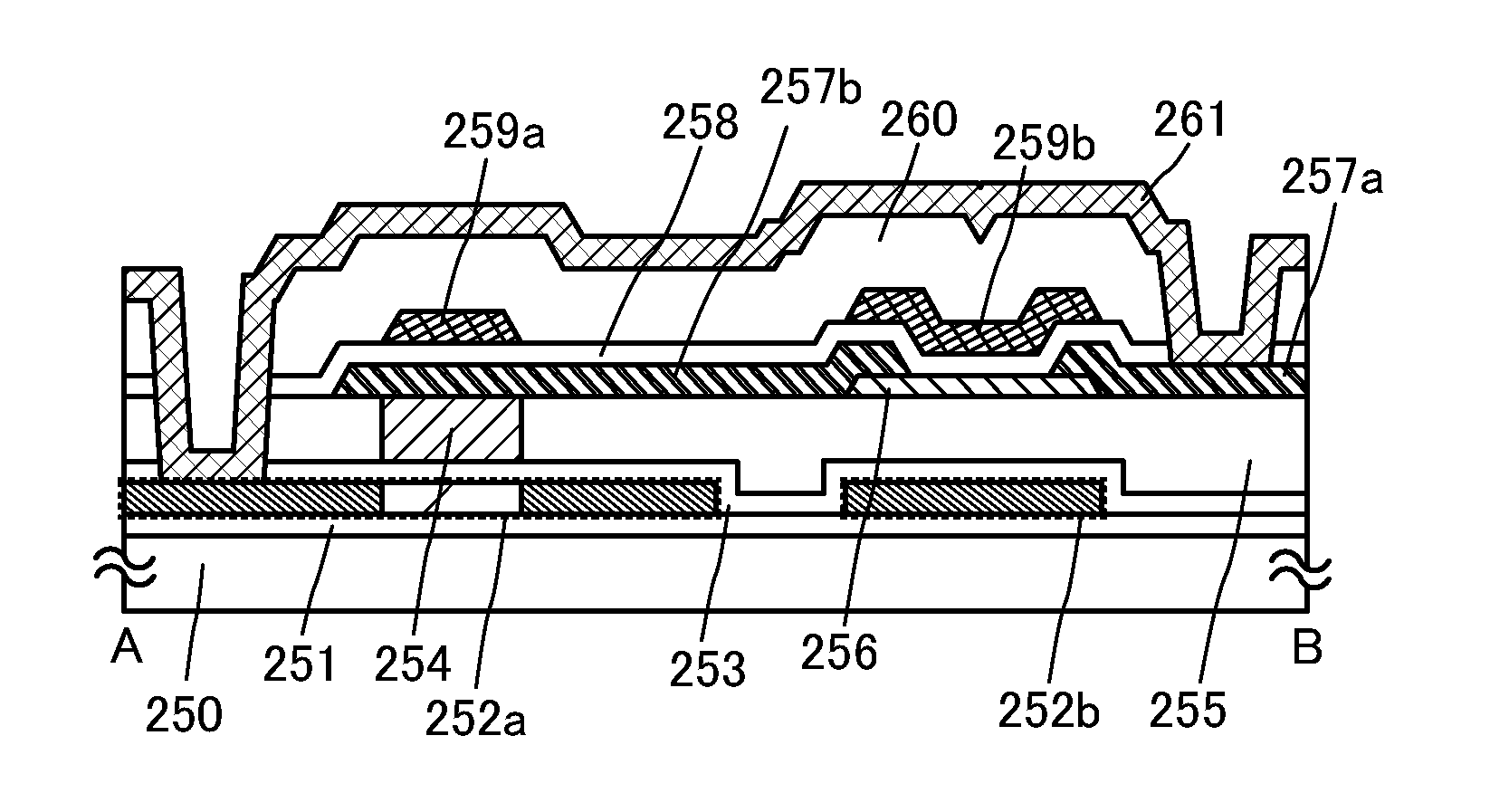
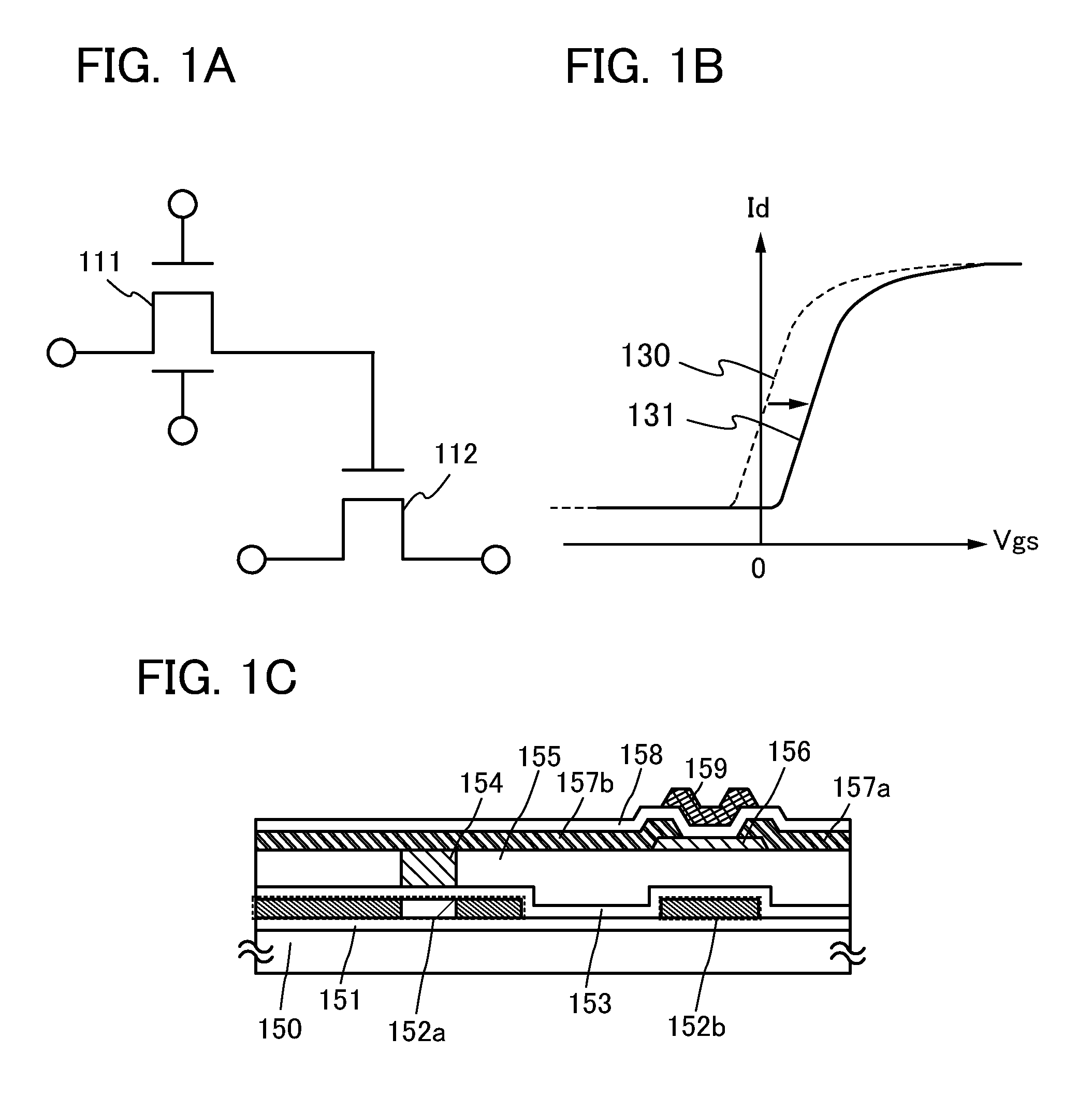
[0035]In this embodiment, an example of a semiconductor device that includes a memory circuit capable of storing data for a certain period is described.
[0036]Note that a memory circuit is a circuit capable of storing electrical charge to be data for a certain period.
[0037]The example of the semiconductor device in this embodiment includes a memory circuit.
[0038]An example of the memory circuit is described with reference to FIGS. 1A to 1C.
[0039]First, a structure example of the memory circuit in the semiconductor device in this embodiment is described with reference to FIG. 1A.
[0040]The memory circuit illustrated in FIG. 1A includes a transistor 111 and a transistor 112.
[0041]Note that in the semiconductor device, the transistor includes two terminals and a current control terminal for controlling current flowing between the two terminals by voltage applied. Note that without limitation to the transistor, in an element, terminals where current flowing therebetween is controlled are ...
embodiment 2
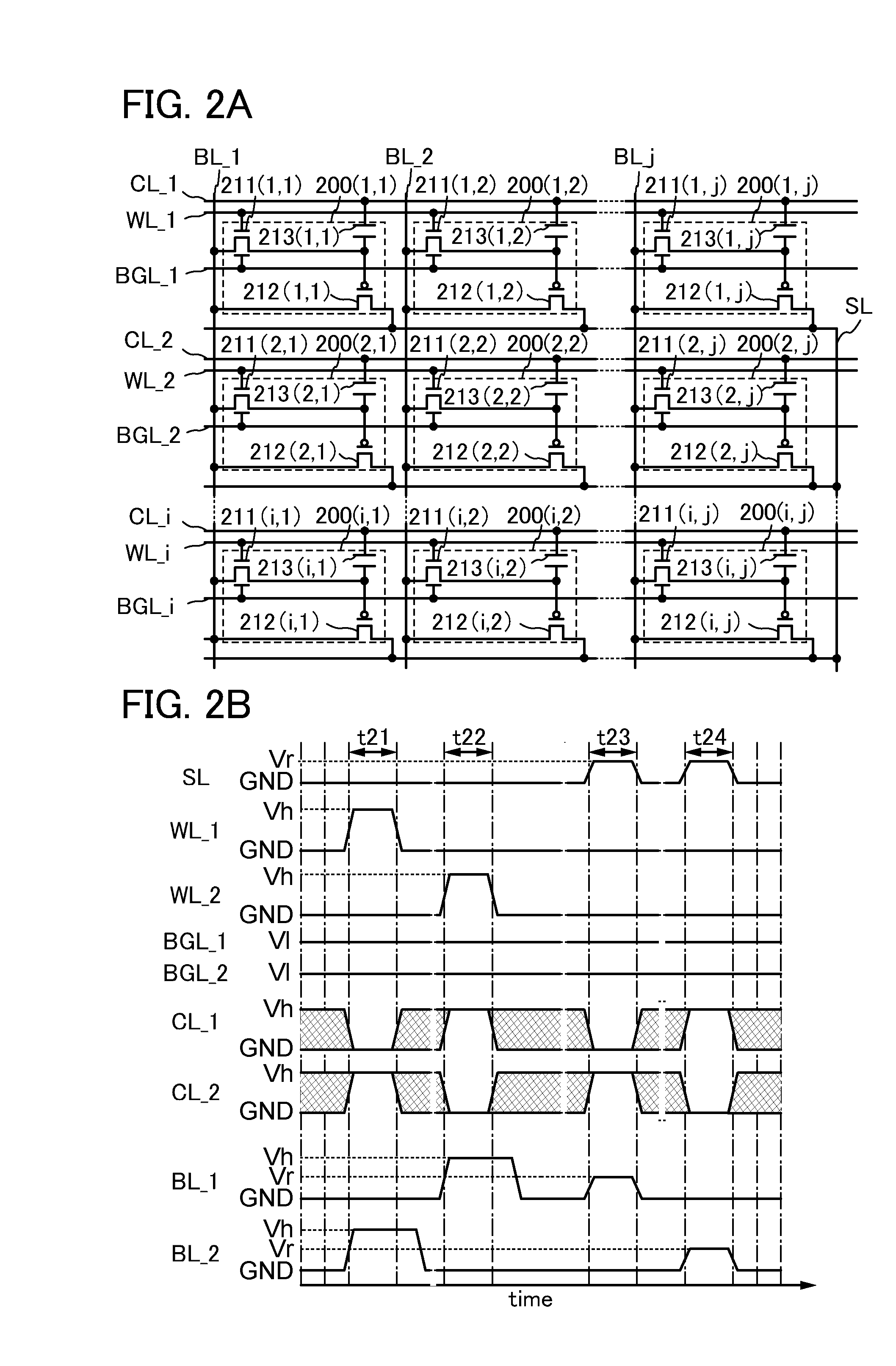
[0115]In this embodiment, an example of a NOR-type semiconductor memory device is described as an example of the semiconductor device in the above embodiment.
[0116]An example of a semiconductor memory device in this embodiment includes a memory cell array including a plurality of memory cells arranged in matrix of I rows (I is a natural number of 2 or more) and J columns (J is a natural number). The memory cell corresponds to the memory circuit in the semiconductor memory device in the above embodiment.
[0117]An example of the memory cell array in the semiconductor memory device in this embodiment is described with reference to FIGS. 2A and 2B.
[0118]First, an example of the circuit structure of the memory cell array in the semiconductor memory device in this embodiment is described with reference to FIG. 2A.
[0119]The memory cell array illustrated in FIG. 2A includes a plurality of memory cells 200 arranged in matrix of i rows (i is a natural number of 3 or more) and j columns (j is a...
embodiment 3
[0258]In this embodiment, an example of a NAND-type semiconductor memory device is described as an example of the semiconductor device in the above embodiment.
[0259]An example of a semiconductor memory device in this embodiment includes a memory cell array including a plurality of memory cells arranged in matrix of I rows (I is a natural number of 2 or more) and J columns (J is a natural number). The memory cell corresponds to the memory circuit in the semiconductor memory device in the above embodiment.
[0260]An example of the memory cell array in the semiconductor memory device in this embodiment is described with reference to FIGS. 8A and 8B.
[0261]First, an example of the circuit structure of the memory cell array in the semiconductor memory device in this embodiment is described with reference to FIG. 8A.
[0262]The memory cell array illustrated in FIG. 8A includes a plurality of memory cells 300 that are arranged in matrix of i rows (i is a natural number of 3 or more) and j colum...
PUM
 Abstract
Description
Claims
Application Information