Optical adhesive film and flat panel display device having the same

a technology of optical adhesive film and flat panel display, which is applied in the direction of identification means, instruments, signs, etc., can solve the problems of low luminescence efficiency and brightness of pdp, consume a large amount of power, etc., and achieve the effect of improving the adhesive strength

Active Publication Date: 2012-05-10
SAMSUNG DISPLAY CO LTD
View PDF3 Cites 27 Cited by
  • Summary
  • Abstract
  • Description
  • Claims
  • Application Information

AI Technical Summary

Benefits of technology

[0009]One or more aspects of the present invention provide an optical adhesive film for improving the ad...

Problems solved by technology

However, the PDP has low luminescence efficienc...

Method used


Image

  • Optical adhesive film and flat panel display device having the same
  • Optical adhesive film and flat panel display device having the same
  • Optical adhesive film and flat panel display device having the same

Examples


Embodiment Construction

[0060]Hereinafter, exemplary embodiments of the present invention will be described in greater detail with reference to the accompanying drawings.

[0061]An active LCD that uses a thin film transistor (TFT) as a switch device is manufactured using a semiconductor manufacturing process, and it is thus difficult to provide a large screen, but has come into widespread use as a display device for notebook computers.

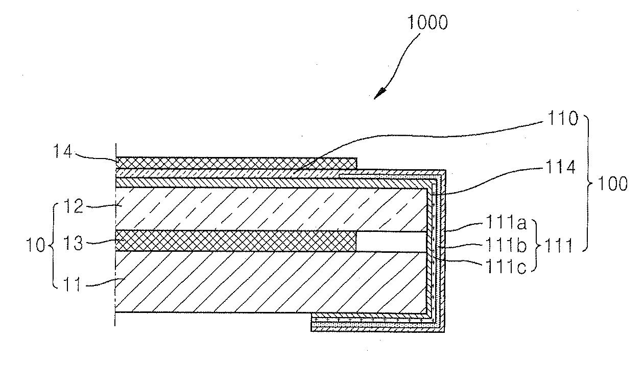
[0062]An LCD is a non self-emitting device, and may include a liquid crystal panel and a backlight unit. The backlight unit is disposed below the liquid crystal panel, and is bonded with the liquid crystal panel via double-faced adhesive tape.

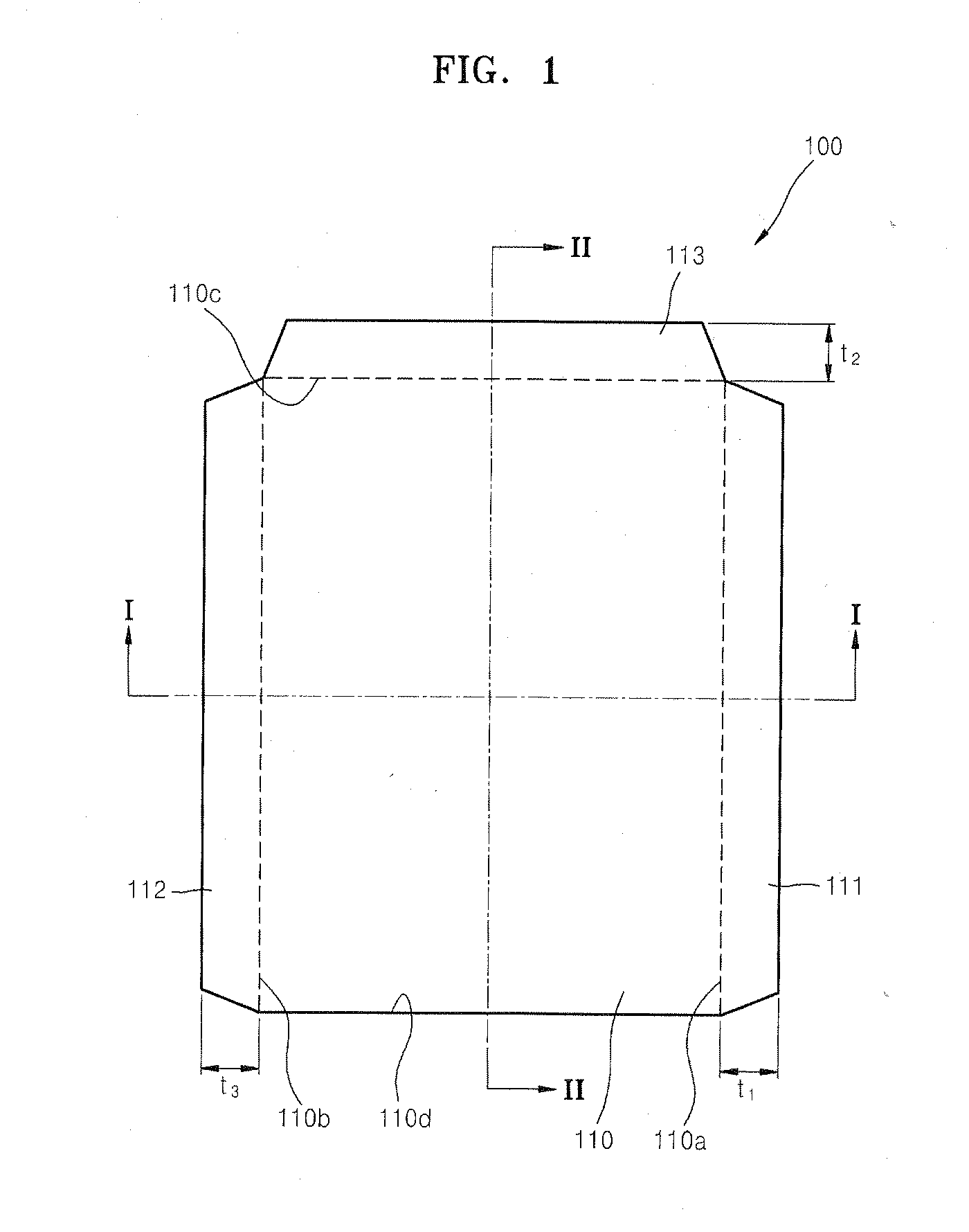
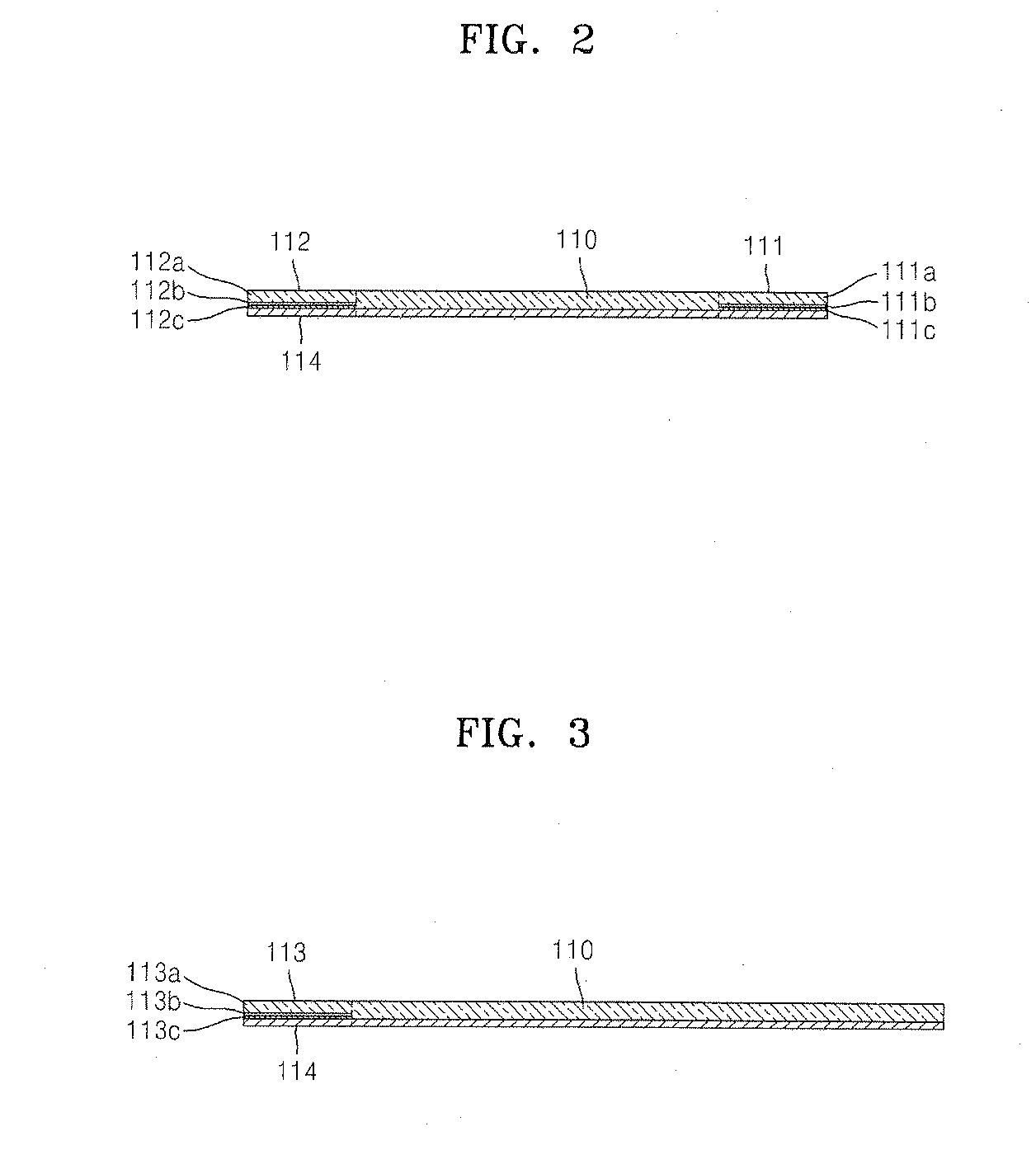
[0063]FIG. 1 is a schematic plane view of an optical adhesive film 100 according to an embodiment of the present invention. FIG. 2 is a cross-sectional view taken along the line I-I of FIG. 1. FIG. 3 is a cross-sectional view taken along the line II-II of FIG. 1.

[0064]Referring to FIGS. 1 to 3, the optical adhesive film 100 includes a tran...


PUM


Abstract

An optical adhesive film for improving the adhesive strength between constitutional elements of a flat panel display device, and a flat panel display device having the same. According to an aspect of the present invention, there is provided an optical adhesive film for use in a flat panel display module that displays an image, the optical adhesive film including a transmission unit disposed on the flat panel display module and allowing the image to transmit through the transmission unit; a wing member extending from at least one side surface of the transmission unit, and covering side surfaces and a portion of a rear surface of the flat panel display module; and an adhesive member disposed covering all surfaces of the transmission unit and the wing member.

Description

CLAIM PRIORITY[0001]This application claims the benefit of Korean Patent Application No. 10-2010-0110996, filed on Nov. 9, 2010 and Korean Patent Application No. 10-2011-0053376, filed on Jun. 2, 2011, in the Korean Intellectual Property Office, the disclosure of which is incorporated herein in its entirety by reference.BACKGROUND OF THE INVENTION[0002]1. Field of the Invention[0003]One or more aspects of the present invention relate to an optical adhesive film and a flat panel display device having the same.[0004]2. Description of the Related Art[0005]Various display devices have recently been developed to replace cathode ray tubes. Examples of such display devices include a liquid crystal display (LCD), a field emission display (FED), a plasma display panel (PDP), and an electroluminescent (EL) display.[0006]From among these display devices, the PDP has drawn much attention since it has a simple structure, and its manufacturing process is considered most suitable to provide a larg...

Claims


Application Information

Patent Timeline
IPC IPC(8): G02F1/1333B32B7/10B32B3/04G02B5/20G02B5/22
CPCG09F3/10G09F7/12G02F1/133308G02F2001/133311Y10T428/24215H01L51/524H01L51/5246H01L51/5271H01L51/5284G02F2202/28G02F1/133311H10K50/841H10K50/8426H10K50/856H10K50/865
Inventor KIM, HWAN-JINHWANG, JEONG-HO
Owner SAMSUNG DISPLAY CO LTD
Why Eureka
Try Eureka