Solid state image sensor

a solid-state image and sensor technology, applied in the direction of material analysis, instruments, radiation control devices, etc., can solve the problems of not being not necessarily satisfactory for improving ranging precision, and not being able to operate satisfactorily for flux separation of off-centered apertures, etc., to achieve the effect of improving the level of ranging precision

Inactive Publication Date: 2012-05-17
CANON KK
View PDF19 Cites 12 Cited by
  • Summary
  • Abstract
  • Description
  • Claims
  • Application Information

AI Technical Summary

Benefits of technology

[0012]Thus, the present invention can provide a solid state image sensor that can operate with an improved level of ranging precision.

Problems solved by technology

However, in a solid-state imaging device according to Japanese Patent Publication No. 3,592,147, the position of the aperture and the position of the pupil of the camera lens are not exactly conjugated and such an off centered aperture cannot satisfactorily operate for flux separation due to scattering of light caused by a wiring section so that the device is not necessarily satisfactory for improvement of ranging precision.
Then, light spreads in the pixel and hence the off centered aperture cannot operate satisfactorily for flux separation.

Method used


Image

  • Solid state image sensor
  • Solid state image sensor
  • Solid state image sensor

Examples


first embodiment

[0061]The first embodiment of solid state image sensor according to the present invention will be described below by referring to the related drawings.

[0062]The solid state image sensor of this embodiment includes a plurality of pixels, each of which has a photoelectric conversion section formed in the inside of a substrate and a light-receiving section formed on the side of a light-receiving surface of the substrate. At least, a part of the plurality of pixels is ranging pixels.

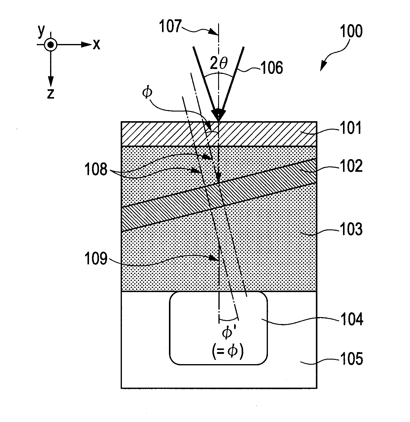
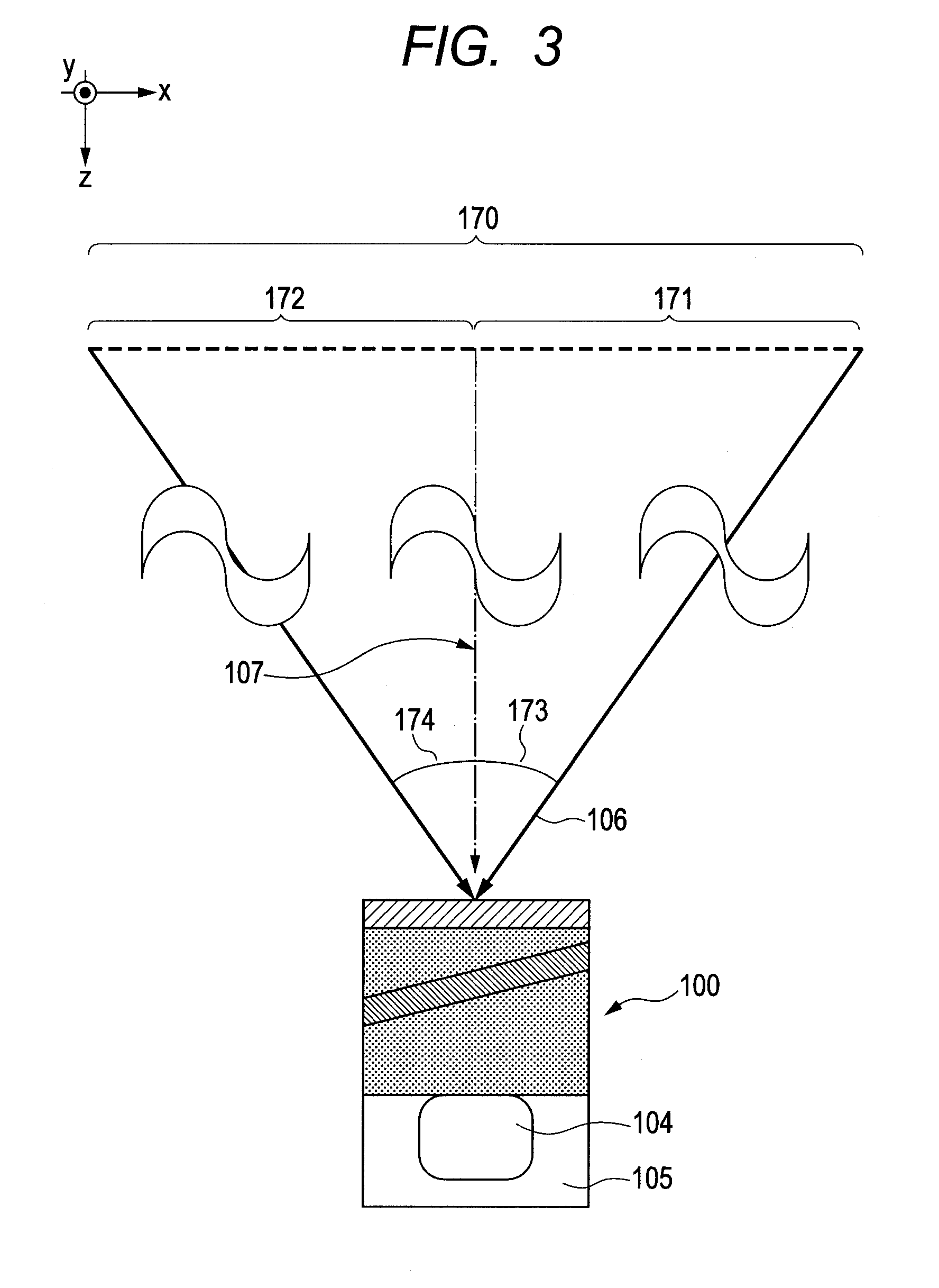
[0063]FIG. 1 is a schematic cross-sectional view of a ranging pixel 100 of the first embodiment.

[0064]Pixel 100 of this embodiment includes a wavelength selective filter 101 that selectively transmits light having the wavelength to be used for ranging operations, a light-receiving section 103 having a guided mode resonant filter 102 in the inside and a silicon substrate 105 having a photoelectric conversion section 104 in the inside arranged in the above mentioned order as viewed from the light-receiving sid...

second embodiment

[0149]The second embodiment of a solid state image sensor having a configuration different from the above-described first embodiment will be described below.

[0150]As seen from FIG. 13, a solid state image sensor 200 of this embodiment differs from the solid state image sensor of the first embodiment in terms of characteristic and arrangement of a guided mode resonant filter 202 and also in that a deflecting element 210 is arranged at the light-receiving side relative to the guided mode resonant filter 202.

[0151]As illustrated in FIG. 14, the guided mode resonant filter 202 is so configured as to represent a characteristic of reflecting incident light inclined by angle γ (predetermined angle of reflection) from the normal line 208 of the guided mode resonant filter 202 with regard to light having the wavelength to be used for ranging operations.

[0152]The guided mode resonant filter 202 is so arranged as to make its normal line 208 agree with the normal line 109 of the silicon substra...


PUM


Abstract

A solid state image sensor includes a plurality of pixels, each having a photoelectric conversion section formed in the inside of a substrate and a light-receiving section formed on the side of a light-receiving surface of the substrate. At least a part of the plurality of pixels is ranging pixels. The light-receiving section of each of the ranging pixels is equipped with a guided mode resonant filter adapted to reflect incident light getting into the inside of the light-receiving section at a specific incident angle. The normal line of the guided mode resonant filter is inclined relative to the principal ray of the flux of light entering the guided mode resonant filter.

Description

BACKGROUND OF THE INVENTION[0001]1. Field of the Invention[0002]The present invention relates to a solid state image sensor. More particularly, the present invention relates to a solid state image sensor to be used for a digital still camera or a digital video camera.[0003]2. Description of the Related Art[0004]Japanese Patent No. 3,592,147 discloses a solid-state imaging device having an image sensor with some of its pixels provided with a ranging function for detecting distances by phase detection as a distance sensing technique for ranging to be used for digital still cameras and digital video cameras.[0005]Unlike conventional contrast measurement systems, the disclosed solid-state imaging device does not need to drive a lens for measuring distances and hence can operate for high precision ranging at high speed. Additionally the disclosed solid-state imaging device can operate for real time ranging when picking up a moving image.[0006]With regard to the structure of the ranging p...

Claims


Application Information

Patent Timeline
Patent Type & Authority Applications(United States)
IPC IPC(8): H01L27/146
CPCH01L27/14621
Inventor NUMATA, AIHIKO
Owner CANON KK
Why Eureka
Try Eureka