Semiconductor package and method of forming the same

a technology of semiconductor chips and semiconductor chips, applied in the direction of semiconductor/solid-state device details, semiconductor devices, electrical apparatus, etc., can solve the problems of electromagnetic interference (emi) generated between the semiconductor chips, the semiconductor chips may generate high temperature when in use, and the semiconductor chips may malfunction

Inactive Publication Date: 2012-05-17
SAMSUNG ELECTRONICS CO LTD
View PDF11 Cites 339 Cited by
  • Summary
  • Abstract
  • Description
  • Claims
  • Application Information

AI Technical Summary

Problems solved by technology

Together with portability of electronic devices, multi-function and mass data transmitting and receiving functions may necessitate complicated printed circuit board designs.
Such semiconductor chips may generate high temperature when in use.
The high temperature may cause malfunctions of the semiconductor chips due to overload.
When a plurality of semiconductor chips are mounted on a printed circuit board, electromagnetic interference (EMI) may be generated between the semiconductor chips.
Such EMI may cause malfunctions of the semiconductor chips.

Method used


Image

  • Semiconductor package and method of forming the same
  • Semiconductor package and method of forming the same
  • Semiconductor package and method of forming the same

Examples


Embodiment Construction

[0041]The inventive concept is described more fully hereinafter with reference to the accompanying drawings, in which embodiments of the inventive concept are shown. This inventive concept may, however, be embodied in many different forms and should not be construed as limited to the embodiments set forth herein. In the drawings, the size and relative sizes of layers and regions may be exaggerated for clarity. Like numbers may refer to like elements throughout.

[0042]As used herein, the term “and / or” includes any and all combinations of one or more of the associated listed items.

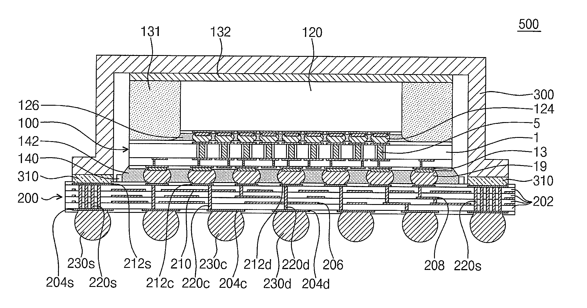
[0043]It will be understood that when an element or layer is referred to as being “on”, “connected to”, “coupled to”, or “adjacent to” another element or layer, it can be directly on, connected, coupled, or adjacent to the other element or layer, or intervening elements or layers may be present. FIG. 1 is a cross-sectional view of a semiconductor package according to an embodiment of the inventive concept.

[00...


PUM


Abstract

Disclosed are a semiconductor package and a method of manufacturing the same. The semiconductor package comprises a package cap which is capable of radiating high temperatures and performs a shield function preventing transmission of electromagnetic waves into and / or out of the semiconductor package. The semiconductor package including the package cap prevents chip malfunctions and improves device reliability. The package cap is positioned to cover first and second semiconductor chips of a semiconductor package.

Description

CROSS-REFERENCE TO RELATED APPLICATIONS[0001]This application claims priority, under 35 U.S.C § 119, from Korean Patent Application No. 10-2010-0114550 filed Nov. 17, 2010, the entirety of which is incorporated by reference herein.BACKGROUND[0002]1. Field[0003]Exemplary embodiments relate to a semiconductor package and a method of fabricating the semiconductor package.[0004]2. Discussion of the Related Art[0005]With trends toward small, slim and dense electronic products, small and slim printed circuit boards are required. Together with portability of electronic devices, multi-function and mass data transmitting and receiving functions may necessitate complicated printed circuit board designs. As a result, there has been an increased need for multi-layer printed circuit boards where power supply circuits, ground circuits, signal circuits, etc. are formed.[0006]Semiconductor chips, such as central processing units, power integrated circuits, and the like may be mounted on multi-layer...

Claims


Application Information

Patent Timeline
Patent Type & Authority Applications(United States)
IPC IPC(8): H01L23/02H01L23/48
CPCH01L21/563H01L23/3128H01L2224/32225H01L2224/29101H01L2924/0665H01L2924/014H01L2924/01075H01L2924/01074H01L2924/01068H01L2924/01033H01L2924/01023H01L2924/01019H01L2924/01006H01L23/367H01L23/3672H01L23/3677H01L23/42H01L23/49827H01L23/552H01L24/29H01L25/03H01L2224/16225H01L2224/2919H01L2224/2929H01L2224/293H01L2224/73204H01L2224/81005H01L2224/92225H01L2225/06513H01L2225/06517H01L2225/06527H01L2225/06555H01L2225/06589H01L2924/01047H01L2924/01049H01L2924/01082H01L2924/01005H01L2924/00H01L2924/14
Inventor IM, YUNHYEOKLEE, CHUNGSUNCHO, TAEJE
Owner SAMSUNG ELECTRONICS CO LTD
Why Eureka
Try Eureka