Semiconductor package with bonding wires of reduced loop inductance

a technology of inductance reduction and semiconductor devices, applied in the field of semiconductor devices, can solve the problems of large noise and jitter of wires

Inactive Publication Date: 2012-05-17
LONGITUDE LICENSING LTD
View PDF2 Cites 7 Cited by
  • Summary
  • Abstract
  • Description
  • Claims
  • Application Information

AI Technical Summary

Problems solved by technology

As the bop inductance between S (signal) and G (ground) wires is large, the wires are subject to large noise and jitter.

Method used


Image

  • Semiconductor package with bonding wires of reduced loop inductance
  • Semiconductor package with bonding wires of reduced loop inductance
  • Semiconductor package with bonding wires of reduced loop inductance

Examples


1st exemplary embodiment

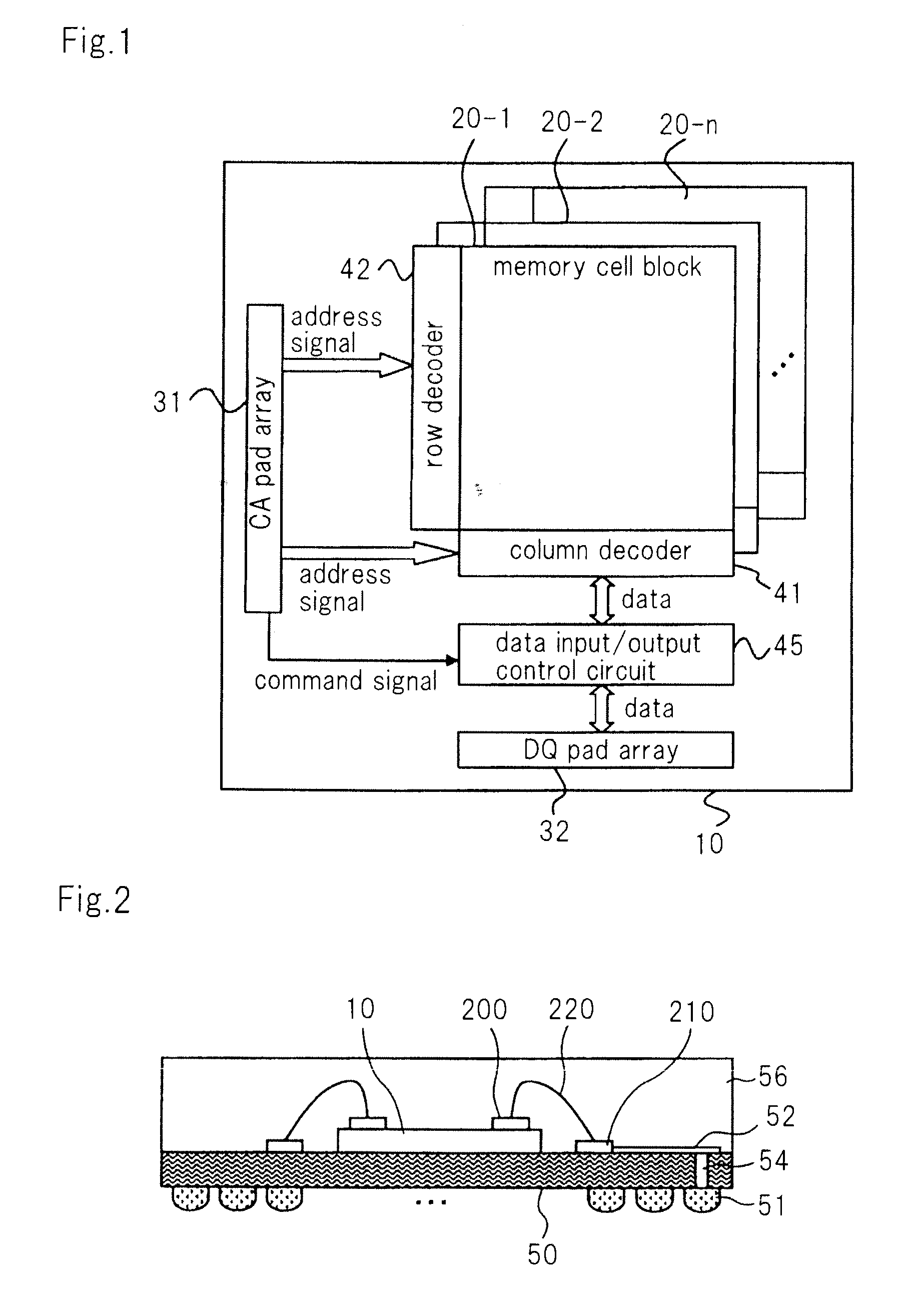
[0041]The structure of a semiconductor package according to the first exemplary embodiment will be described below. FIG. 5 is a plan view illustrative of a structural example of a central portion of the semiconductor package according to the first exemplary embodiment.

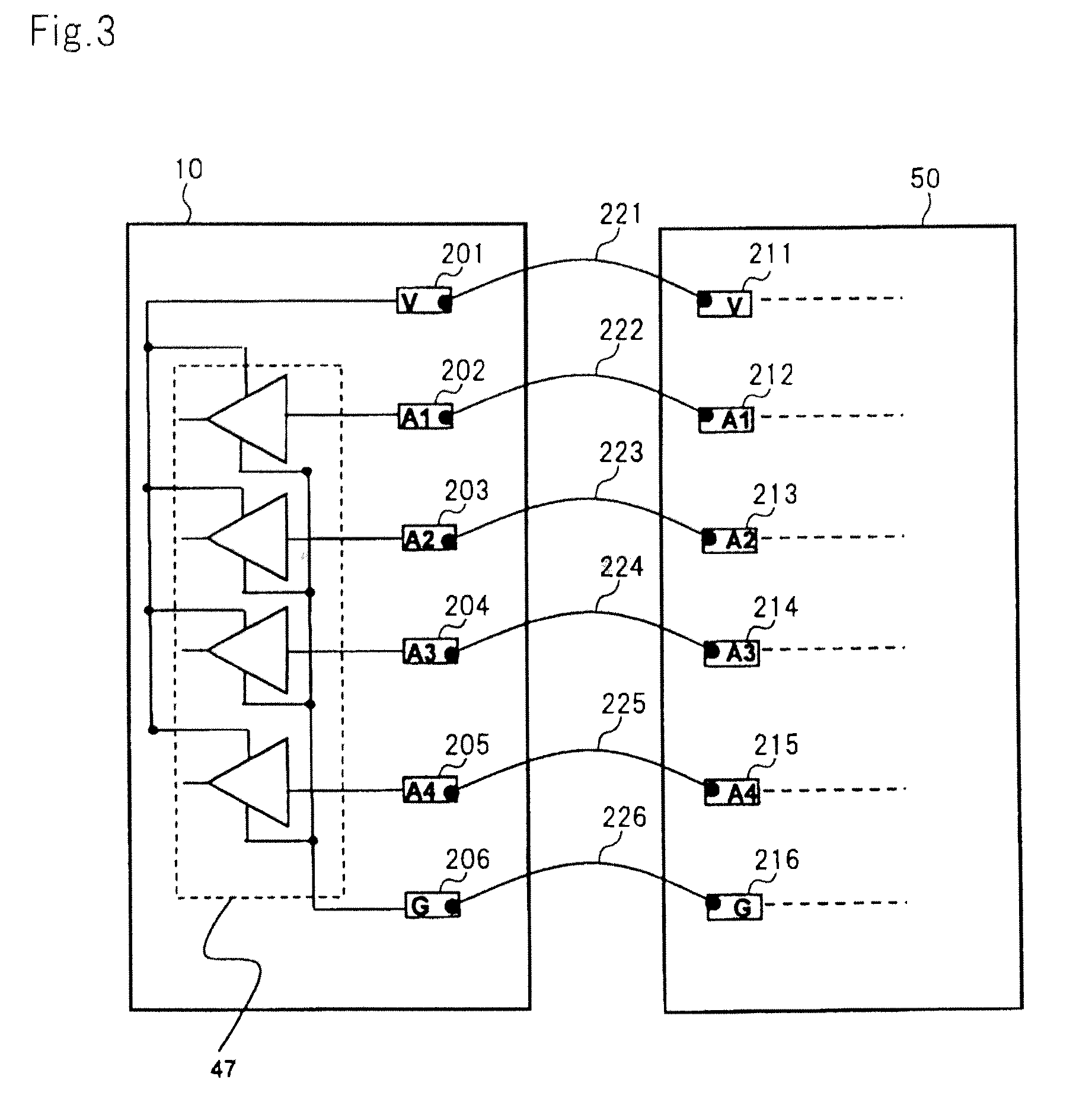
[0042]FIG. 5 shows connections between pads on semiconductor device 12 and bond fingers on package board 60. It is assumed that horizontal directions in FIG. 5 are referred to as X-axis directions and vertical directions as Y-axis directions. Semiconductor device 12 has the structure shown in FIG. 1. The structural details shown in FIG. 1 will not be described below, and those details of semiconductor device 12 which are different from those shown in FIG. 3 will be described below.

[0043]Semiconductor device 12 is mounted on package board 60. In FIG. 5, a portion of package board 60 is shown separately to clearly illustrate connections between pads on semiconductor device 12 and bond fingers on package board 60. A plana...

example 1

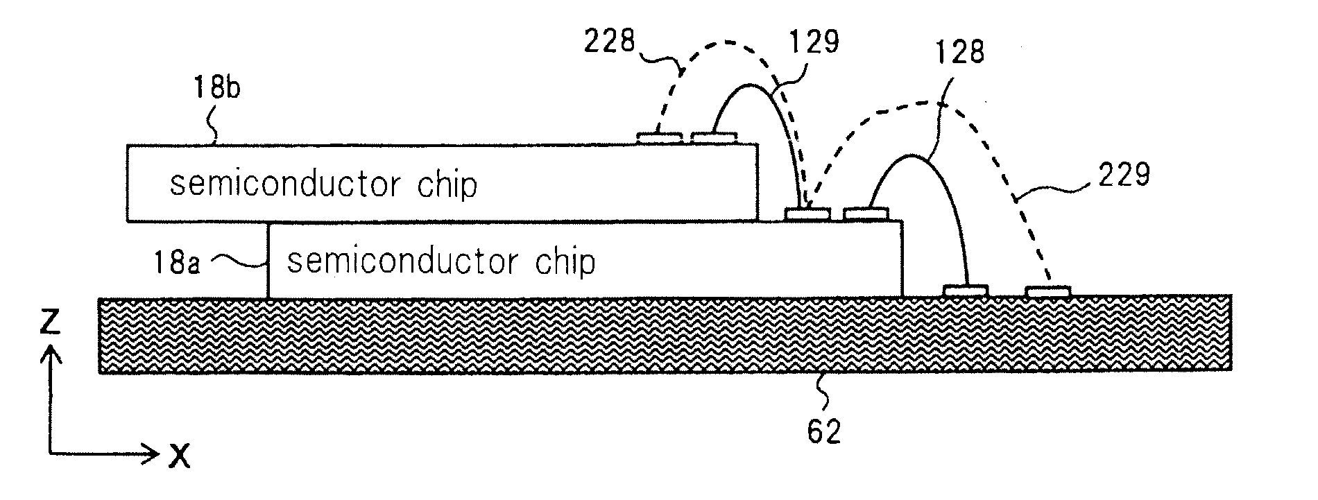
[0087]The present example is concerned with a semiconductor package having a PoP structure in which two semiconductor devices are stacked on a package board.

[0088]The structure of the semiconductor package according to the present example will be described below. FIG. 10 is a plan view of the semiconductor package according to the present example, and FIG. 11 is a side sectional view of the semiconductor package according to the present example. In FIGS. 10 and 11, a resin body which covers semiconductor chips is omitted from illustration. It is assumed that horizontal directions in FIG. 10 are referred to as X-axis directions, vertical directions as Y-axis directions, and directions perpendicular to the principal surface of package board 62 as Z-axis directions.

[0089]As shown in FIG. 11, semiconductor chip 16a and semiconductor chip 16b are successively stacked on package board 62. Each of semiconductor chips 16a, 16b is a DRAM chip. As shown in FIGS. 10 and 11, semiconductor chip ...


PUM


Abstract

A semiconductor package includes a semiconductor device including a plurality of signal pads and a plurality of auxiliary pads which are alternatively arranged in a predetermined direction, and a package board including a plurality of signal bond fingers, a plurality of first power supply voltage bond fingers, and a plurality of second power supply voltage bond fingers. The signal pads are connected respectively to the signal bond fingers by first wires. The first power supply voltage bond fingers and the second power supply voltage bond fingers are connected respectively to the auxiliary pads by second wires. The first wires are disposed between those of the second wires which are connected to the first power supply voltage bond fingers and those of the second wires which are connected to the second power supply voltage bond fingers.

Description

[0001]This application is based upon and claims the benefit of priority from Japanese Patent Application No. 2010-252913 filed on Nov. 11, 2010, the content of which is incorporated by reference.BACKGROUND OF THE INVENTION[0002]1. Field of the Invention[0003]The present invention relates to a semiconductor package including a semiconductor device mounted on a package board.[0004]2. Description of the Related Art[0005]The structure of a semiconductor package including a semiconductor device will be described below. First, the structure of the semiconductor device will be described below. FIG. 1 of the accompanying drawings is a block diagram showing a structural example of semiconductor device 10 according to the related art. It is assumed that semiconductor device 10 is a DRAM (Dynamic Random Access Memory).[0006]As shown in FIG. 1, semiconductor device 10 includes a plurality of memory cell blocks 20-1 through 20-n (n represents an integer which is 1 or greater) each including a pl...

Claims


Application Information

Patent Timeline
Patent Type & Authority Applications(United States)
IPC IPC(8): H01L23/50H01L23/522
CPCG11C5/06H01L2224/05553H01L24/05H01L24/06H01L24/49H01L25/0657H01L2223/6611H01L2224/05013H01L2224/48091H01L2224/48137H01L2224/48145H01L2224/48227H01L2224/49175H01L2224/49176H01L2224/49431H01L2225/06506H01L2225/0651H01L2225/06527H01L2924/01013H01L2924/014H01L23/525H01L2224/04042H01L23/498H01L2924/30107H01L2224/48463H01L2924/01033H01L2924/01023H01L2924/0102H01L2924/01005H01L2924/00014H01L2924/00H01L2924/181H01L2924/15173H01L24/48H01L2224/45099H01L2924/00012
Inventor KATAGIRI, MITSUAKIIWAKURA, KENUEMATSU, YUTAKA
Owner LONGITUDE LICENSING LTD
Why Eureka
Try Eureka