Wiring board, method for manufacturing same, display panel, and display device
a technology for wiring boards and display panels, which is applied in the direction of resistive material coating, cable/conductor manufacturing, printed circuit non-printed electric components association, etc., can solve the problems of unfavorable corrosion of metal wires, and achieve the effect of preventing metal wire corrosion or braking
- Summary
- Abstract
- Description
- Claims
- Application Information
AI Technical Summary
Benefits of technology
Problems solved by technology
Method used
Image

Examples
embodiment 1
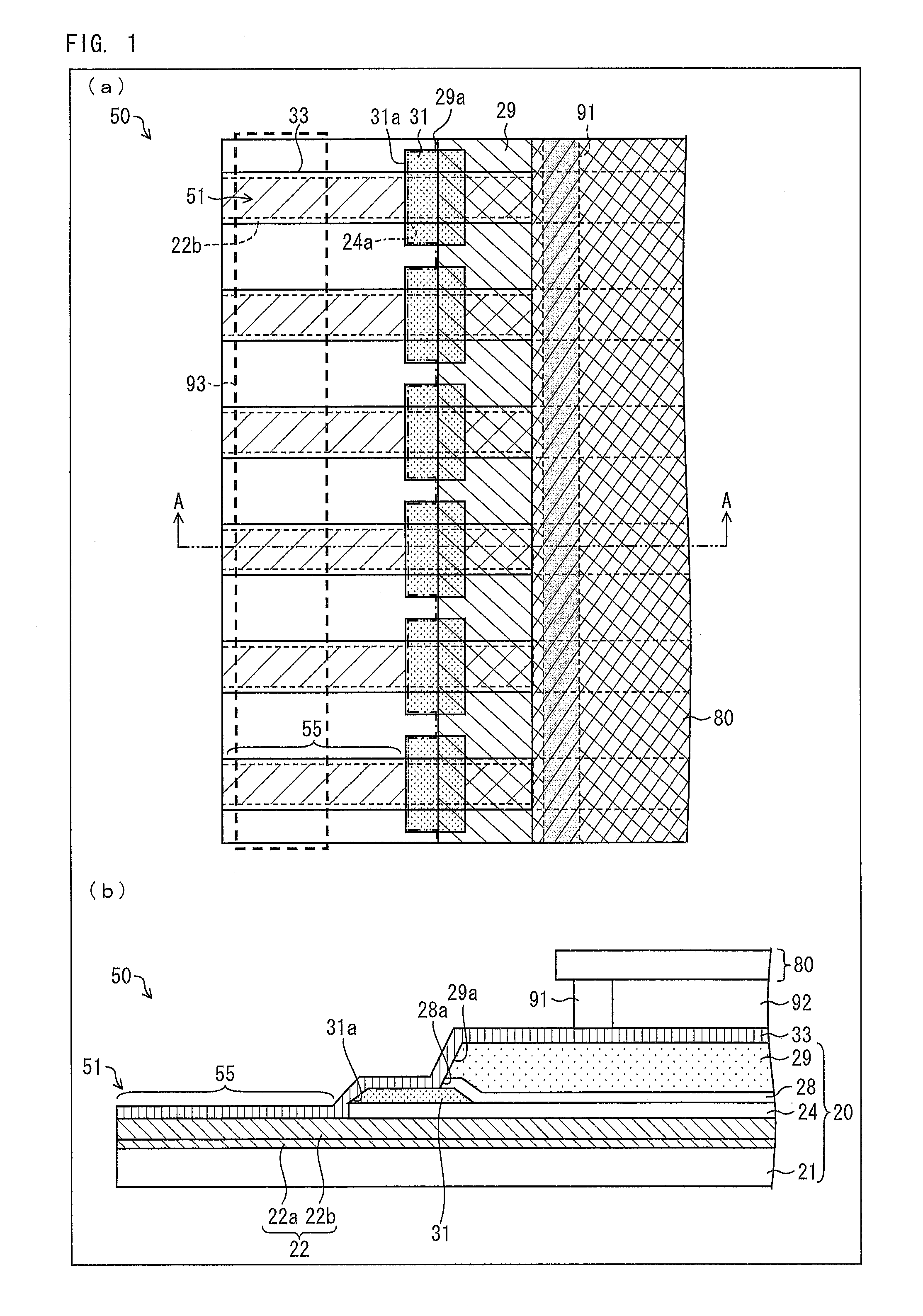
[0066]An embodiment of the present invention is described below mainly with reference to (a) and (b) of FIG. 1 through (a) and (b) of FIG. 7, FIG. 19, and FIG. 20.
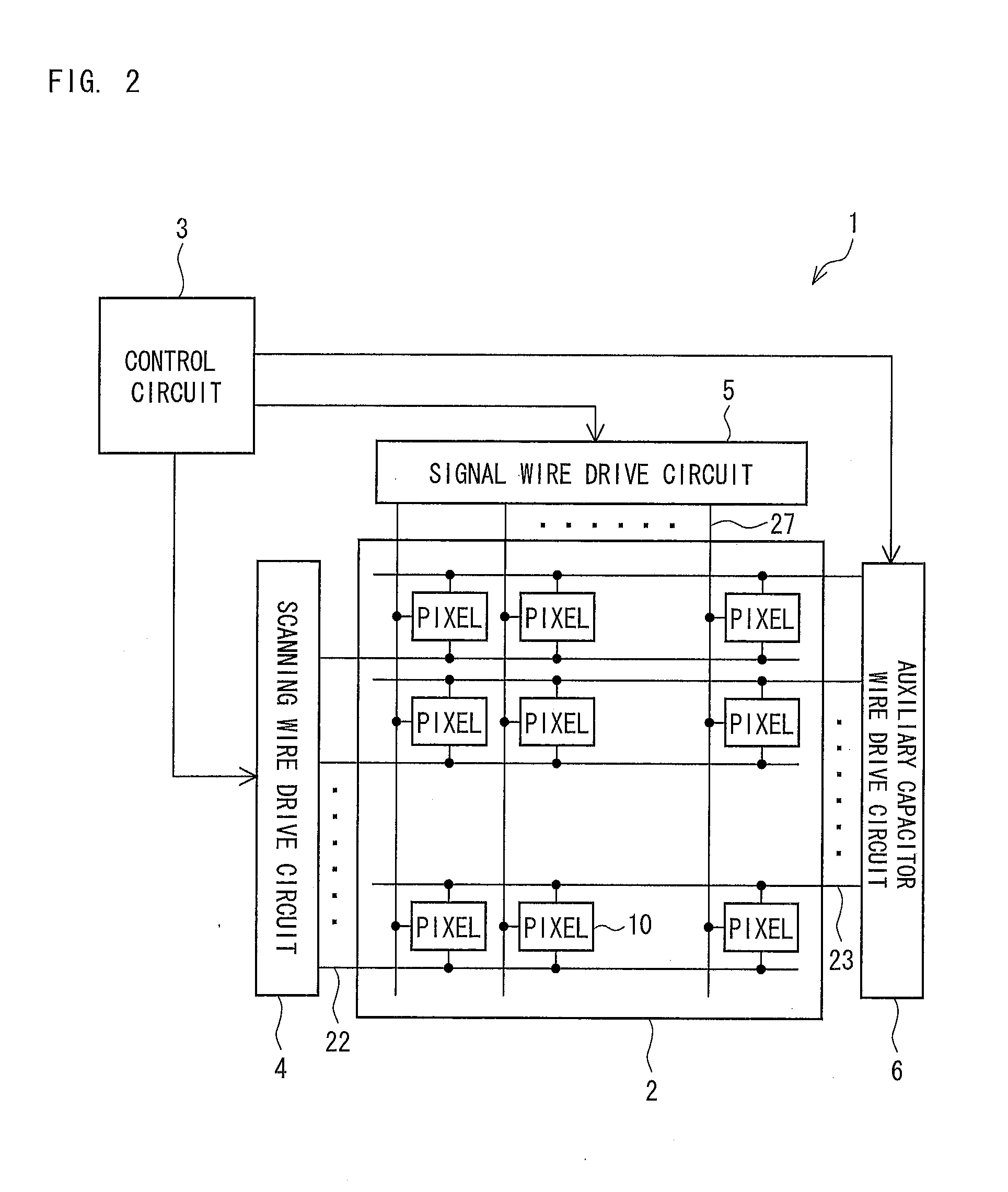
[0067]FIG. 2 is a block diagram schematically showing a configuration of a main part of a liquid crystal display device according to the present embodiment.
[0068]As shown in FIG. 2, a liquid crystal display device 1 according to the preset embodiment includes: a liquid crystal panel 2 (display panel), on which pixels 10 are arranged in a matrix manner; a drive circuit, which drives the liquid crystal panel 2; a control circuit, which controls driving of the drive circuit; and, as needed, a backlight unit (not illustrated), etc.
[0069]The liquid crystal panel 2 is provided with a plurality of scanning wires 22 and a plurality of signal wires 27 each intersecting with each of the scanning wires 22, and has a pixel 10 (pixel section) provided for each combination of a scanning wire 22 and a signal wire 27. Further, the liquid ...
embodiment 2
[0241]Another embodiment of the present invention is described below with reference to FIG. 8. It should be noted that in the present embodiment, points of difference between the present embodiment and Embodiment 1 are mainly described, and that those components having the same functions as those of Embodiment 1 are given the same reference numerals, and as such, are not described below.
[0242]As with Embodiment 1, the present embodiment is described by taking the scanning wire connection area 50 as an example of the connection area 44. However, the scanning wire connection area 50, the scanning wires 22, the scanning terminals 51, and the scanning electrodes 12 can be read as the signal wire connection area 60, the connection wires 62, the signal terminals 61, and the signal electrodes 13, respectively. Further, in the auxiliary capacitor wire connection area, too, a similar reading is possible, with changes made only in the names of the metal layers (wires).
[0243]FIG. 8 is a plan v...
embodiment 3
[0249]Another embodiment of the present invention is described below with reference to (a) and (b) of FIG. 9. It should be noted that in the present embodiment, points of difference between the present embodiment and Embodiment 1 are mainly described, and that those components having the same functions as those of Embodiment 1 are given the same reference numerals, and as such, are not described below.
[0250]As with Embodiments 1 and 2, the present embodiment is described by taking the scanning wire connection area 50 as an example of the connection area 44. However, the scanning wire connection area 50, the scanning wires 22, the scanning terminals 51, and the scanning electrodes 12 can be read as the signal wire connection area 60, the connection wires 62, the signal terminals 61, and the signal electrodes 13, respectively. Further, in the auxiliary capacitor wire connection area, too, a similar reading is possible, with changes made only in the names of the metal layers (wires).
[0...
PUM
| Property | Measurement | Unit |
|---|---|---|
| surface roughness | aaaaa | aaaaa |
| thickness | aaaaa | aaaaa |
| thickness | aaaaa | aaaaa |
Abstract
Description
Claims
Application Information
 - Generate Ideas
- Intellectual Property
- Life Sciences
- Materials
- Tech Scout
- Unparalleled Data Quality
- Higher Quality Content
- 60% Fewer Hallucinations
Browse by: Latest US Patents, China's latest patents, Technical Efficacy Thesaurus, Application Domain, Technology Topic, Popular Technical Reports.
© 2025 PatSnap. All rights reserved.Legal|Privacy policy|Modern Slavery Act Transparency Statement|Sitemap|About US| Contact US: help@patsnap.com